The pricey promise of microLEDS
A pixel used to be just a colored dot on a digital picture. In its latest avatar, the pixel is morphing into a multitalented minion capable of emitting light, recording fingerprints, sensing 3D motion, or even performing respectable calculations using integrated circuits.
To be clear, the pixel has not grown larger in size. It continues to shrink along with all the devices it decorates. But instead, the area required for emitting light within the pixel has shrunk, freeing enough real estate to onboard additional functionalities.
This remarkable transformation is mainly due to microLEDs, a display technology poised to enter adulthood after many adolescent years spent in research labs. Tech giants such as Microsoft, Google, Facebook, Intel, Apple, and Samsung are gobbling up small startups and medium-sized companies working in this space. There has been an uptick in the number of patents and scientific publications on microLEDs in the past few years: interest and activity are palpable.
The field has come a long way since 2017, when the Samsung Wall was introduced as one of the first microLED TVs. It had a whopping 146-inch display consisting of 66 million pixels that delivered an unprecedented 16K resolution. It cost around $100,000.
Four years later, microLED displays continue to be expensive, which inhibits adoption for everyday personal devices. And they're expensive because it's technologically challenging to arrange them into a display.
"Assembly is the most significant challenge for microLED technology," says John Rogers, director of the Querrey-Simpson Institute for Bioelectronics at Northwestern University. He has pioneered scalable approaches to microLED assembly, specifically for flexible and wearable devices.

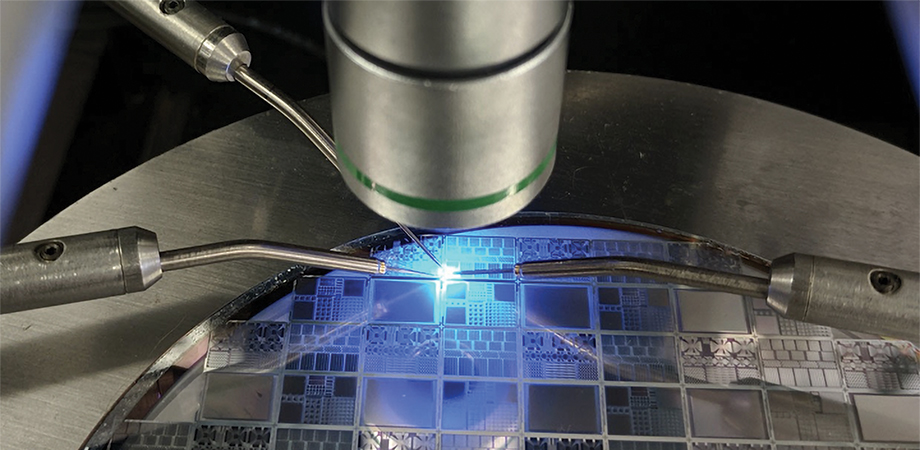
Samsung's "The Wall" MicroLED Display debuted in 2017. Credit: Courtesy of Samsung
Ioannis (John) Kymissis, department chair and the Kenneth Brayer Professor of Electrical Engineering at Columbia University, agrees: "The primary drivers for cost are putting all the parts together—which could be hundreds of thousands of components."
Along with his recent graduate student, Keith Behrman, Kymissis has worked extensively on microLEDs, and is a founder of Lumiode, a startup that works on a class of microdisplay elements for augmented reality (AR) applications.
"The first [mass market] applications for microLEDs will be in small displays such as smartwatches and AR glasses," Behrman says, "and that's because they are extremely bright." Pausing, he adds, "In fact, per unit area, they are as bright as the surface of the Sun." To clarify, the comparison is with the Sun as we see it in the sky, but that's still incredible.
"AR displays need high luminance as the waveguided optics are typically lossy, reducing the effective brightness," Behrman continues. It's this high luminosity that makes microLEDs attractive for small displays such as smartwatches and wearable devices that need to convey information on a limited area, often in competition with ambient light.
LEDs exist on a continuum of sizes. Yole Développement, a semiconductor market research firm in France, labels anything larger than 200 µm as a macroLED, and anything below 50 µm as a microLED. The intermediate size range—between 50 µm and 200 µm—is the domain of the miniLED.
A microLED is therefore the size of a large bacteria or a grain of pollen.
Behrman, however, puts the upper limit of microLEDs at 100 µm. "There is no consensus on the correct definition of a microLED," he says. This confusion also extends to nomenclature. In scientific literature, they are variously referred to as microLED, µ LED, micro-LED, or micro LED.
MicroLEDs often work in the indium gallium nitride compound semiconductor family. The result is a bright blue light that can be easily converted to lower frequency colors such as red and green. This is called down conversion. "It's much easier to down convert from higher frequencies than to up convert from lower frequencies of light. That's another reason why gallium nitride is used in microLEDs," Behrman says.

A scanning electron micrograph of individual microLED pixels showing the isolation and contact features. Credit: Keith Beherman, Columbia University
A single microLED is a small square of gallium nitride (GaN) attached to a substrate. The process of making these structures creates atomic-level imperfections, leading to many incomplete or "dangling" bonds at the edges. "In these regions, electrons and holes undergo nonradiative coupling—that is, they do not produce light when they fuse, thus wasting current. As the LED gets smaller, the ratio of the perimeter to surface area gets larger, creating more dangling bonds," Behrman says.
The small GaN structure is also stretched by the atomic lattice of the substrate, which causes stress that changes the frequency of the emitted light.
The net result of both effects is that the efficiency of microLEDs saturates beyond some value of current density, which is current divided by surface area.
MicroLEDs tend to carry very large current densities. "Because the current density can be as much as 10,000 times higher, the peak luminance is also higher," Kymissis says. That's why microLEDs are so dazzlingly bright.
"The small sizes also allow for better heat dissipation," adds Rogers. "Inorganic materials such as gallium nitride are much more chemically and thermally stable compared to organics. A powerful consequence is that microLEDs do not need sophisticated encapsulation strategies, thereby providing a very straightforward pathway to flexible, and even stretchable... displays," Rogers comments.
MicroLED displays therefore consist of individual LEDs directly attached to a backplane that contains all the electronics (including transistors) that control when the LED is turned on/off. However, given their small size, the sheer number of microLEDs required for a display is staggering.
A 4K display refers to a screen resolution of 3840 2160, or roughly 8.3 million pixels. A market report from Yole notes that making a 4K microLED display is tantamount to "assembling 25 million grains of pollen with a positioning accuracy of 1 micrometer, without a single error." This helps explain why assembly is so challenging. In addition, each pixel needs to switch between red, green, and blue lights.
This color-switching can be done in one of two ways. The first method is to fabricate separate microLEDs for each of the three colors of light and assemble them together on the backplane. The second is to assemble only blue LEDs on the backplane and cover them with a multicolored filter that will convert blue to the other two colors.
Like other semiconducting devices, microLEDs are made in clean rooms. They are made by the thousands on a wafer, and need to be carefully transferred to the backplane. Given that it takes millions of microLEDs to form a single display, it is impractical to transfer them one at a time.
Instead, LEDs are mounted first onto smaller transfer stamps that shuttle them in batches to the backplane. Consider a 12.5 12.5 mm2 transfer stamp—10,000 transfer cycles would be needed to populate a 75-inch TV panel. The process needs to be repeated three times if the colors are being assembled separately. A larger transfer stamp of size 102 100 mm2 would only need 170 transfer cycles for the same job.
Yole has suggested adding an "interposer" to this process. Smaller transfer stamps will print LEDs to an intermediate transfer stamp, which will then carry over to the display. It's really the same problem as when there are more people who need to travel than there are vehicles to accommodate them. The key is efficient batching or rideshares.

A passive matrix microLED display developed at Columbia University for use in miniature microscopes for animal studies. Credit: Keith Behrman, Columbia University
Kymissis has been working with displays where the chiplets have a lot of space in between. Since microLEDs are very bright, the spacing does not affect the quality of the display but does allow for the transfer to be faster while allowing for more functionalities to be added to the screen. "You typically want the display to be on the order of 100 to 1,000 nits of luminance on the order of your TV or smartphone. The chiplets themselves are much brighter, so they are spread out and the rest of the display is available as a dark background to increase contrast, carry electronics, be transparent," and so on, he says.
Smaller displays such as those used for projectors and AR/VR glasses will continue to use closely packed microLEDs. Kymissis continues "The microdisplays are much brighter—10 to 50 million nits."
Although transfer stamps streamline the transfer to the display backplane, the microLEDS first must be moved from the growth wafer to the stamp.
That's an area that Rogers has worked on a lot. The system that he uses for retrieving and printing the microLEDs involves, quite literally, a rubber stamp—a very high resolution, precision stamp, with tiny, raised features that match some multiple of the pitch of the LEDs on the source wafer. He explains that there are two parts to the transfer process: fabrication and undercut release of fully formed microLEDs from the source growth wafer, and physical mass transfer using stamps to target substrates. Both operations are now fully developed and refined to manufacturing standards.
Rohinni, a 25-member microLED company started in 2013, has patented a unique cartridge printer method for chiplet transfer. The process resembles traditional newspaper printing, where a drum prealigned with LEDs is rolled on the backplane. As the surface rolls over it, the chiplet sticks to the display, held by weak forces of attraction.
Startup eLux, based in Vancouver, Washington, has perhaps the most novel technique of all. They have patented a self-assembled microLED display where the individual chiplets float in a solution and fall into the correct position by gravity.
It's too early to say if any of these processes will lead to less expensive microLED displays. That will require them to be industrially scaled and evaluated. However, given the inherent complexity and the number of steps involved in each method, there is a chance for an error to creep in. This reduces the yield, or the number of working microLEDs that have survived the transfer process. As Kymissis points out, "Yield and quality issues are also paramount in many microLED applications, and techniques and technologies for improving yield and productivity are something to keep an eye out for."
In the life cycle of a microLED, a defect can arise as scratches or pits in the initial growth process, during etching, while transferring, or through the interconnects that power them. A 2018 Yole report analyzed the challenge of repairing dead LEDs in a 4K panel. Even if the fabrication process has a yield of 99.99 percent, that still leaves 2,500 dead pixels on the screen. This can easily take a couple of hours to find and fix during production.
And that's assuming that the LED can be repaired at all. Typical microLEDs are encased in a protective layer and coated with an electrode on the top, and an elaborate backplane at the back. Most often, it's not even clear where the defect is, let alone being able to fix it.
Unfortunately, as Behrman points out, our eyes will notice even a single dead pixel on a screen. That makes a 4K display with 99.99 percent yield undesirable.
For that reason, both Kymissis and Behrman think that micro-LEDs are likely to be adopted by microdisplays long before macrodisplays. "Microdisplay applications are still emerging commercially but have been in intense development for AR/VR, automotive lighting such as active headlights, and projector applications," Kymissis says. "Smartphones, for example, are not a good first target for microLED displays. I am confident that we will see both existing and new markets addressed through microLEDs."
Rogers, however, is far more optimistic about the impending ubiquity. "MicroLED technology is poised to dominate all forms of displays. Particularly exciting unique applications are in transparent display, flexible display, stretchable display for skin-integrated devices, and many others."
Vineeth Venugopal is a scientist and science writer who loves all things and their stories.
| Enjoy this article? Get similar news in your inbox |
|


