Gambling with chips: New metrology tools reduce the odds for error in electronic devices
Without metrology, semiconductor manufacturing is a gamble with chips.
A typical microchip fabrication process involves up to 1,000 different steps, multiple materials, and can take anywhere from a week to a month. The result is a tiny silicon wafer with billions, even trillions of transistors patterned onto it with military precision, often to the specification of a few atoms.
“At every step of this, we need to ask, “Are you sure?’” says Andy Antonelli, senior director of R&D and Fellow at Onto Innovation, a leading semiconductor process control company.
By that he means repeatedly inspecting the wafer after every critical processing step, making sure that the wafer is even, that the materials have been laid down smoothly, that the patterns have been etched accurately, and that there is not even a speck of dust anywhere in the nanoscale megacity that is a modern microchip.
“In the old days, all you needed was an optical microscope,” says Alain Diebold, professor emeritus and Empire Innovation Professor of Nanoscale Science at SUNY Polytechnic Institute and author of the Handbook of Silicon Semiconductor Metrology.
However, as Moore’s law pushes transistors down to the size of a few atoms, metrology has become ever more critical, and equally challenging. As deep UV immersion lithography at 193 nm wavelength gives way to extreme UV lithography (EUV) with a 13.5 nm wavelength, the size of the smallest etch pattern has shrunk from 40 nm to about 9 nm. At this scale, quantum mechanics and statistics come together to create chaos, resulting in random patterning errors that are not well understood and hard to eliminate.
While shrinking in size, device structures are becoming increasingly complex. A 3D NAND (three dimensional not-AND) device used in the latest flash drives can be made of 32 to as many as 128 layers of materials and be 20-µm tall—a true skyscraper inside a microchip. These contain a 20-nm contact hole that needs to be precise and extremely vertical, something akin to a mineshaft. Measuring a structure with this unusual aspect ratio is challenging, to say the least.
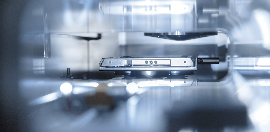
A new set of optical tools and techniques are helping to push metrology into this bold new domain of ultralow dimensions. However, for these instruments to do so, visible light is increasingly being replaced with invisible infrared, ultraviolet, and X-rays. Simple optical microscopes are giving way to advanced analytical devices that use complex computation and machine intelligence to function. These include, for example, newer iterations of optical critical dimension (OCD) metrology; critical dimension small angle X-ray scattering (CDSAXS); multibeam electron microscopes, and Mueller matrix spectroscopic ellipsometry.
While they are built to serve a new generation of lithographic techniques, they fundamentally have the same goal as all metrology systems that came before them: establishing control and confidence in the microchip manufacturing process.
“Measurements start at the wafer level. A 300-mm wafer is a sizable thing to be cut out from a silicon boule,” says Diebold, referring to the single, cylindrical crystal of ultra-pure silicon that is the starting point for all integrated circuits. Different manufacturers will have different requirements for the smoothness, thickness, and bow and warp of the wafer that need to be verified.

Caption: Concept drawing of a large array of micro-electron beam columns scanning a wafer surface in parallel. With this embodiment, the columns could either be controlled individually or collectively, depending on the inspection requirements. Photo Credit: Bradley Thiel
The purity and specificity of all gases, chemicals in wet etches, sputter targets, metals, and dopants need to be checked. And while patterning, the dimension and shape of all etch structures must be verified.
And finally, the patterned wafer must be checked for defects. This could be anything from a stray particle of dust or a bit of photoresist that gets left behind in a pit, to a pattern that did not print correctly or smoothly enough.
Each of these measurement systems belongs to one of three categories: dimensional, material, or defect metrology. While common tools such as the ellipsometer can perform more than one type of measurement, specialized tools are needed for other measurements.
The most common method for dimensional analysis is an ellipsometer. A detector measures the reflection of a beam of light off a surface. The incident light is polarized, with its electric field pointing in a specific direction. The rotation of the electric field caused by material characteristics of the reflecting surface allows, through analysis at different wavelengths, determination of the surface’s precise thickness, crystalline structure, chemical composition, roughness, dopant concentration, and electrical conductivity.
Where it gets challenging is when a complicated structure like the skyscraper 3D NAND device needs to be measured. That’s when advanced tools like OCD metrology become useful. “An OCD is basically an ellipsometer,” says Antonelli. “Only the analysis is more complicated.”
To wit: The reflection pattern of a simple thin film is easily understood when measured with an ellipsometer, but a complex shape has a more intricate reflection pattern, making it challenging to decipher the polarization pattern.
To meet that challenge, tools like Onto Innovation’s OCD start by modeling what the ellipsometric response of a given structure should be using first-principle, physics-based computation, and then compare the response with experimental observations. If the two patterns match well, then there is confidence in the etched design. Any deviation suggests that there is a change from the expected design and consequently, an error. In particular, if a midinfrared wavelength between 5 to 12 µm is used for the OCD, it is found to work well with 3D NAND structures and for contact channel measurement.
However, for OCD to work, the opto-electronic response of all the materials used in the device must be well known. Specifically, this means that the refractive index and the dielectric dispersion—two key properties of light—must be known for every wavelength in the measurement range.
As the semiconductor industry innovates and experiments with new materials, this information is often not available. Sometimes, assumptions are made in the computational model. Other times, the material response should be determined before modeling.
At the US National Institute of Standards and Technology (NIST), materials scientist R Joseph Kline is developing CDSAXS, an advanced version of critical dimension metrology that uses X-rays and is similar to protein crystallography. It works by shining a beam of X-rays at a 50- to 100-µm spot within a microchip device. Repeating patterns, such as protein crystals or a regularly spaced array of patterned devices, diffract light in specific ways and result in definite but abstract diffraction patterns.
Like the OCD measurement system, the expected diffraction pattern for a given design is computed ahead of time and compared with experimental observation. If there is a deviation, the model is tweaked repeatedly until the two patterns match.
Kline calls CDSAXS a “volume-weighted measurement,” which means it assesses the average performance of a device structure, rather than identifies individual errors within a pattern. Its strength lies in an ability to quickly detect irregularities in a pattern during production, rather than identifying isolated errors. It’s the difference between finding a single black spot on a white T-shirt versus a line of spots. So, for example, CDSAXS might not be able to pick up a single misprinted spot in a pattern but can flag when there is a repeated misprint.
As device patterns continue to shrink, identifying individual errors within becomes increasingly difficult. With EUV lithography, for example, an etched line is only about 20 nm in dimension, and with a recommended tolerance of 20 percent, the maximum variation in thickness can be no more than ±5 nm. This presents a significant metrology challenge.
Typical lithographic processes transfer a pattern from a mask to the silicon wafer by using a light-sensitive material called a photoresist. The wafer is coated with the photoresist and then exposed to light through the mask. The light causes a chemical reaction in the photoresist, which hardens or dissolves depending on the type of photoresist used. After the exposure, the substrate is then developed, which washes away the areas of the photoresist that were exposed to light.
For example, a series of rectangles can be created on a wafer by using a mask with rectangular holes to project UV light onto the photoresist. This hardens the photoresist into rectangular films that survive the washing process. When the wafer is etched, the areas outside of the rectangles are removed, leaving raised rectangles on the surface of the wafer.
While each chip maker may have its own photoresist formula, the basic ingredients are typically a polymer, a sensitizer, and a solvent. When exposed to light and developed, the photoresist produces precise and sharp features essential to silicon lithography.
As the size of etched features continues to shrink, however, there are fewer photoresist molecules directly above the etch region, posing two main challenges: The number of photons of light that reach this region becomes small and uncertain, and there may not be enough photoresist to initiate the photochemical reaction needed for the etching step.
As a result, the etching process can become a random event. “Occasionally, there may be an unusual clustering or dispersal of photoresist molecules in a specific area,” says Gregory Denbeaux, an associate professor of nanoengineering at SUNY Polytechnic Institute. This can affect the final dimension and shape of the etched pattern, potentially leading to wider or narrower patterns than expected.
These random errors, so-called stochastic errors, in EUV lithography can negatively impact the overall performance of microchips. When even one transistor operates at a slower clock speed, it can result in decreased performance for the entire chip.
The key to understanding stochastic errors—rare but vital-to-detect phenomena—is to establish statistical bounds. Do they happen once in a million or a billion etch steps? That’s where fast, accurate, and precise metrology becomes important. “How can you know that [the stochastic error rate] is less than a billion if you have not measured a billion?” asks Denbeaux.
And because they are rare and could be anywhere on the whole wafer, there can be extreme difficulty scanning for stochastic defects.
In fact, Bradley Thiel, professor of nanoengineering at SUNY Polytechnic Institute, says, “Finding these defects is like looking for five blades of brown grass in a football stadium from the press box at night.”
Thiel says the only way to accurately find them might be with a now commercially available technique for defect detection that he helped develop: multibeam electron microscopy.
As an electron beam is charged, it functions like a multimeter, measuring the local electrical properties of the device and creating a comprehensive electrical map of the pattern. The small wavelength of an electron beam allows it to accurately image defects, provided they can be located in the first place. With a single beam and a scan area as large as a full wafer, this can take many months.
Multibeam electron microscopy, on the other hand, significantly accelerates the scanning process by projecting hundreds of beams onto one area simultaneously. Along with speed of defect detection, this makes it useful for tracking stochastic defects in EUV technology.
Zeiss has a 91-beam electron tool. But the technology is evolving and there could soon be an even larger number of beams available for scanning. And that could ensure that defects are found faster, no matter how rare and how small.
Kline believes that as lithographic technology advances, the complexity of device structures will pose a greater challenge than size. With the increasing use of 3D structures and new materials in devices, for example, next-generation metrology systems must be able to accurately map and inspect each layer of those complex devices.
Metrology is a growth industry, says Antonelli. “Anyone can come up with a fantastic new transistor, but without metrology they wouldn’t be able to make it trillions and trillions of times.”
We still need metrology to double-check and ensure the reliability of the semiconductor manufacturing process by asking the all-important question, “Are you sure?”
Vineeth Venugopal is a science writer and materials researcher who loves all things and their stories.
| Enjoy this article? Get similar news in your inbox |
|


