Silicon Lasers: the Final Frontier
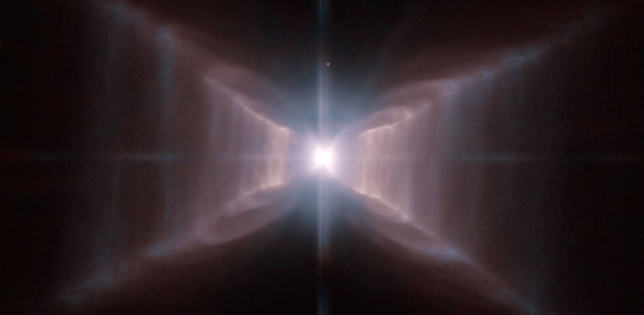
The Red Rectangle is one of the weirdest objects in the Universe. For one, it is a rectangle—a highly unusual shape for an enormous cloud of gas. Second, long jets of gases extend diagonally across the nebula to form a giant X, as if the Universe itself had crossed it off a long time ago. Third, its eerie red glow is attributed to silicon that has been crushed into fine nanoparticles.
These crystals emit a diffuse band of red light that spans wavelengths from 500 to 800 nm. Early measurements pointed to a rather high photoluminescence with quantum yields between one and ten percent. When announced in the 1990s, these results were not just incredible, they seemed impossible.
Silicon, it was well known, is an indirect bandgap semiconductor. Excited electrons in silicon produce heat, not light. It was just not possible for this material to emit light, certainly not at the yields that were being reported.
Three decades later, a high-yield silicon light source remains elusive on Earth. An LED or laser made wholly from silicon has the potential to radically transform microchips of the future, enabling light-speed processing as well as massive energy savings. In fact, a silicon laser has become so sought after that it has been described as the "final frontier" and the "holy grail of optoelectronics." However, despite concerted efforts by the photonics community, a satisfactory silicon laser has not yet been developed.
In spite of silicon's lackluster photonic properties, this unassuming semiconductor has some extraordinary achievements. By the last decade of the last millennium, silicon had spawned the biggest technological upheaval since the industrial revolution. Transistors, microchips, and integrated circuits made from silicon made possible small, affordable, and energy-efficient devices that could execute complex tasks. This proliferation of computing devices has in turn enabled communication and knowledge generation at unprecedented rates.
Along with all that increased data traffic comes heat, which has become a pressing engineering problem to solve. The constant movement of electrons through the tiny metal highways inside a microchip leads to pernicious Joule heating. This is of particular concern for the large data centers that run the internet. Anywhere from 35 to 65 percent of the total expense in running a data center is spent on cooling. It is no wonder, then, that many data centers are located in cold places like Alaska and Ireland. There was an urgent need to solve the "heat problem," though it wasn't clear what that would look like.
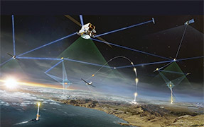
By the early 2000s, an active community of researchers was exploring ways to use light to transmit information between and within microchips. Their goal was to eliminate electrical interconnects within a chip altogether, replacing them with optical waveguides that carry information encoded on photons. The challenge is to create systems that can produce, transport, and modulate light at the scale of a microchip, using techniques that are compatible with current technology. At the end of the last millennium, none of these things existed.
That's why the strangest thing about the discovery of silicon nanocrystals in a nebula was its timing. The broadband emission from the Red Rectangle seemed to portend a technological revolution brewing here on Earth, with silicon once again at its heart.
Removing the Data Communication Bottleneck
In the last 20 years, a number of novel discoveries have propelled silicon photonics—the study and application of photonic systems that use silicon as an optical medium—into the mainstream. High-precision etching technology has created silicon waveguides that are the same size as the wavelength of light it carries. These structures have made it possible to transfer information from one part of the chip to another without any heat or hassle.
Along with the waveguides came optical modulators, oscillators, and resonators that could precisely modify the properties of light. On-chip spectrometers have become available that can extract molecular and atomic signals from incident light on a device that is smaller than a fingernail.
These photonic devices have an enormous range of potential applications. The most consequential is the replacement of integrated circuits (ICs) that run on electrons with photonic integrated circuits (PICs) that run on photons. The best case would be a fully integrated silicon photonic circuit with no electronic components whatsoever. The next best option is a hybrid silicon photonic circuit that coexists with electronic transistors. To match the high production volume and low-cost efficiency of the current generation of microprocessors, these photonic circuits would have to be compatible with CMOS fabrication technology.

An artistic rendering of a waveguide-coupled ring cavity. Credit: Bahram Jalali
"Huge increase in data traffic demands PICs or integrated photonic chips. The carrier of data in PIC is light," said Ming Lu, professor in the Department of Optical Science and Engineering at Fudan University. "The preferred choice of silicon PICs is to grow all the necessary photonic elements on a silicon-based wafer, in a way that matches the process flow of silicon-based microelectronics."
Bahram Jalali, director of the UCLA Photonics Laboratory, concurs: "This will remove the data communication bottleneck and enable massively distributed computing."
There is, however, one component that stands in the way of a fully integrated silicon photonic circuit: a reliable source of light that can fit onto a microchip.
Most photonic circuits and devices today use an external source of light, usually a III-V compound semiconductor laser that is mounted on the microchip or connected via a fiber optic cable. These GaAs or InP lasers are very useful in a lab because they are efficient and highly reliable. However, it is challenging to scale them towards large-scale commercial production.
The ideal scenario for silicon photonics is a light source made from silicon. Such an LED or laser can be easily integrated on a chip and be readily fabricated. According to Jalali, "Being able to mass manufacture lasers using silicon foundries would be a game changer."
The diffuse light from the Red Rectangle seems to suggest that this bright silicon future should be possible, where high-efficiency devices proliferate on low-cost photonic chips.
However, the fundamental obstacle towards this photonic future is the indirect band gap of silicon. What this means is that an excited electron in silicon cannot return to the ground state without a push from somewhere - usually through lattice vibrations called phonons.

Luminescent porous silicon. Inset: TEM image confirming crystallinity and photoluminescent colloidal suspensions. Credit: Leah Canham
It's not very hard to excite electrons in silicon—any blue laser will do the job. However, these electrons will wait for a phonon to come along, which can take somewhere around 10 to 30 milliseconds. By this time, the wandering holes and electrons in silicon would have combined with the defects in the crystal lattice to produce heat, not light.
In fact, a million electrons need to be excited in silicon to generate a single photon. By comparison, GaAs only requires two excited electrons per photon. To summarize, silicon can emit light, but with very small yields.
A way out of this conundrum was suggested in 1990 by Leigh Canham, then affiliated with the Royal Signals and Radar Establishment. He showed that crystalline silicon with over 80 percent porosity showed photoluminescence in the red when exposed to diffuse blue light.
"I had been recruited in 1986 to develop silicon light-emitting diodes and had been trying to use light-emitting defects in bulk silicon. Nano structuring was a route to dramatically increase exciton binding energy by quantum confinement," Canham recalls. "Porous silicon was available, being studied for other reasons, and I could see a way to get quantum wires from it by further etching." His intuition was correct: the nanowires could be coaxed into photoluminescence.
This work led to many low-dimensional silicon systems, including nanocrystals, semiconductor-insulator superlattices, and nanopillars being actively investigated as a means of improving the light-emission properties of silicon.
Among those actively investigating silicon as a light source was Lorenzo Pavesi, the current head of the NanoLab at the University of Trento. He and his collaborator, Francesco Priolo, understood that the lesson from porous silicon is that nanostructuring leads to an improvement of the optical gain.
In 2000, Pavesi and Priolo showed that the optical efficiency of nanocrystals made from annealed silicon oxide was 10,000 times better than bulk silicon. An effective nanocrystal light emitter has a size that is comparable to the wavelength of electrons in it. For silicon, this is around 3 to 5 nm. At this size, the holes and electrons are constrained within the structure, decreasing the recombination time from milliseconds to microseconds. During recombination, these charge carriers have a much higher chance of creating a photon than heat. Further, these crystals have reduced defects, limiting another source of carrier depletion.
This principle is exactly how the nanocrystals in the Red Rectangle were able to produce light. It just so happens that the nebula managed to do this with no formal training in quantum mechanics, millions of years before we set out to do the same.

The red square is a silicon LED on a chip which emits red light following electrical injection. Credit: Lorenzo Pavesi
The next big step towards a silicon laser, however, came from an unexpected direction. In 2003, Jalali and his team at UCLA developed a Raman silicon laser. This is widely considered to be the first true silicon laser. Like porous and nanocrystalline devices, these lasers also required a light source for excitation. However, this light interacts with phonons in silicon to excite light emission through the Raman effect. The Raman lasers from Jalali's group only produced intermittent pulses of light. The first continuous silicon Raman laser was created in 2005 by a team at Intel led by Haisheng Rong. These lasers were made from a narrow silicon waveguide cut into a dielectric medium.
The Raman laser proved conclusively that an indirect band gap does not prohibit lasing action. "Raman lasers are used for wavelength conversion. They have special applications in scientific, military, and medical fields," Jalali explains. However, they are not fully compatible with silicon PICs for a number of reasons, the need for an optical pump among them. He continues, "My main goal was to prove that textbooks are wrong and that silicon can amplify light and lase very efficiently."
Despite these advances, no silicon laser or LED has been able to match the optical gain of III-V lasers. This has led some to question whether a fully silicon light source is either practical or desirable. As Jeff Shainline, staff scientist at the National Institute of Standards and Technology, Boulder, puts it, "None of the light sources match the performance of compound semiconductors, and most of them don't solve the problem of integration with microelectronic circuits." He and many others think that a better solution would be to figure out how to integrate III-V lasers with silicon.
Integrated or External Light Source?
In recent years there has been some progress in this direction. John Bowers at the University of California, Santa Barbara, has shown that it is possible to bond GaAs and InP to a silicon wafer. There are still challenges to solve, such as growing a 300 mm III-V wafer that is compatible with CMOS. If a silicon laser does not materialize, this might be our best shot at integrated silicon photonics.
However, silicon light sources continue to be an active area of research. In 2018, Ming Lu and his collaborators at Fudan University improved on the work of Pavesi by creating a nanocrystal silicon laser with improved optical gain. They did this by greatly increasing the concentration of nanocrystals in their material. Like the previous lasers, their laser is also optically pumped. However, Lu says, "We are now working on an electrically pumped silicon laser that should be of practical use in developing silicon PIC."
It is important for a PIC-compatible silicon laser to be electrically pumped. Otherwise, these devices will need to carry an external light source, which brings us back to the problem that we set out to solve: a fully silicon PIC.
At the same time, new and creative applications for photonic chips are constantly being explored. One such system is the development of neuromorphic circuits in silicon that mimic the interaction of neurons in our brain. This is one of problems that Shainline is trying to tackle. "Photonic circuits might be the only way to implement these neurons in the billions, as observed in biological systems," he says.
It's too early to tell where the red light from the Red Rectangle will lead us. Will silicon lasers become a reality, or will they be an interesting detour in the development of integrated III-V lasers on silicon? Or, will the ideal light source for the photonic circuits of the future be found elsewhere?
Vineeth Venugopal is a scientist and science writer who is passionate about all materials and their stories.
| Enjoy this article? Get similar news in your inbox |
|