Neural Networks Help Chip Manufacturing
Neural networks may detect killer defects

By mimicking how people learn, researchers hope to improve chip manufacturing. The promise can be seen in presentations at the SPIE Advanced Lithography symposium on machine learning. Further research and development is needed to account for specific and specialized requirements. One is that there must never be a false negative - for example, classifying a chip or mask as good when, in fact, it has not.
Neural net technology could be used to optimize mask layout, according to Woojoo Sim of Samsung. In a talk on Tuesday 26 February, he discussed lithographic hot spots. These are regions in a chip layout where, for instance, the tips of two lines come close together. While not a violation of design rules, a narrow gap increases the likelihood of bridging and a killer defect.
The traditional methods to locate such hotspots leave something to be desired. "They are expensive because they take many days," Kim said.
In fact, the scanning run time may be weeks, he added. Additionally, traditional methods often overcorrect, making changes where none are needed. This happens because the algorithms think there is a problem where there is not.
Seeking a better solution, a research team from Samsung, the University of Michigan, and Brown University turned to neural networks, a technique that learns what the differences are between objects called good and those deemed bad. Once trained, a neural net can then classify new objects, such as a layout, as either good and bad. This capability can then be used to correct a layout, turning it from bad to good.
The researchers followed this model, giving their system a few thousand images of layouts with and without hotspots. Once that was complete, they tested it on other layouts, achieving good success in finding and fixing hotspots without excessive correction.
Further research will apply the technique to more complicated hotspot situations, such as when neighboring lines are wide or long. The technique is not computationally taxing, according to Kim. So, it could be applied more widely to layouts than current methods.
Another application of neural nets involves finding defects, the subject of a presentation by Bryan Barnes of the National Institute of Standards and Technology (NIST). The task is challenging because feature sizes continue to get smaller at the same time chips are increasing in complexity.
"It requires constant innovation," Barnes said of defect detection in a talk on Wednesday 27 February.
The best solutions are optical because they allow entire wafers to be scanned, he said. But that is difficult because the defects may be much smaller than the wavelength of light. What's more, this defect scanning takes place across a patterned surface. This can help some wavelengths and hurt others, depending upon the wavelength in comparison to the pitch, the center-to-center feature spacing.
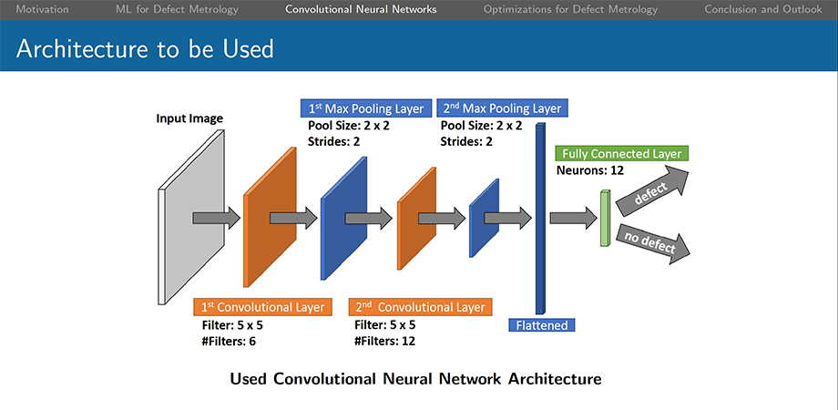
For instance, studies at NIST indicate that when the pitch of a line array is about 100 nm, 193-nm light works well for inspection. However, it is hard to spot a defect using a wavelength around 150-nm. To minimize this effect and ensure the greatest flexibility in exploitable wavelengths, the NIST team turned to neural networks, using a set of simulated images for training and another simulated set for evaluation of the resulting classifier.
They were able to get good results, but more research needs to be done. For instance, where should the dividing line be in terms of neural net output between good and bad?
An important point in setting this threshold and evaluating it, Barnes said, is that not all classification errors are of equal economic impact. There can be false positives, where the neural net thinks there is a defect when there isn't. In that case, more inspection may be done, costing money and time. However, the other error is a false negative, a case where the neural net thinks there is no defect when there is.
Generally, the semiconductor industry wants the chance of this to be zero because of the fear of a killer defect getting through. "You don't want false positives, but you really don't want false negatives," Barnes said.
Hank Hogan is a science writer based in Reno, Nevada.
See more news and highlights from SPIE Advanced Lithography.


