Driving Moore’s Law into the next decade
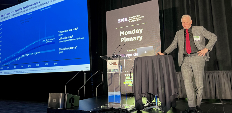
During a talk that opened the 2023 Advanced Lithography + Patterning conference, Martin van den Brink, president and CTO of lithography equipment maker ASML, took a look at the past and the future. He first touched on a presentation he gave in 2008 that discussed how the industry might continue to enhance lithography, thereby shrinking chip features and boosting device performance.
“Now I’m sitting here 15 years later, and I still believe we will still continue to shrink lithography,” van den Brink said.
Such progress is critical for future semiconductor advances. These innovations have historically led to newer chips performing more operations per second for less energy than their predecessors. Every two years, chips have become roughly four times as efficient, allowing people today to walk around with more storage in a phone that fits in a pocket than was used to go to the Moon 50 years ago.
In his most recent presentation, van den Brink, as he had done in 2008, touted holistic lithography. This concept encompasses the lithography and patterning that produce chip features, the metrology that measures the results of that process, the optimization of transistor, chip, or system that maximizes what can be achieved, and more.
New technology and tools are helping improve holistic lithography. For example, van den Brink noted that local variation of individual nanometer-sized features plays a large role in setting an overlay budget, the amount by which a new layer can be misplaced relative to a previously printed layer. To maximize overlay, engineers take into account nearby features to tweak shapes on a photomask so that what is printed at the end of the patterning process is as close as possible to what was originally intended.
Known as optical proximity correction or OPC, this technique results in odd shapes. It can be difficult and time consuming to develop models of what corrections to make in the dense circuitry of a chip.
Using deep learning to ingest and analyze large data sets enables engineers to come up with better models for this optical proximity correction in a shorter time. “It’s saving us,” van den Brink said.
Looking to the future, he mentioned the need to deploy both high and possibly even hyper-NA EUV. Extreme ultraviolet, or EUV, lithography is critical in making the most advanced chips because it can print smaller features more cost effectively than alternatives.
All EUV systems have a numerical aperture, or NA. A higher NA means a system has greater resolution and is therefore able to print smaller features. Today’s EUV standard is an NA of 0.33. Systems with 0.55, or high, NA are going into wafer fabs and will soon be involved in producing chips. On the horizon is 0.75 or higher NA technology, or a hyper NA EUV.
However, van den Brink noted that in his 2008 talk he spoke of high NA EUV systems. Moving these into high volume production has not taken place yet, in part because of the need to develop masks, photoresists, and more to support the technology. That infrastructure is now arriving. But the infrastructure for hyper NA is not here yet, and so ASML and others are researching and developing it.
There also is work underway to roll out metrology advances, improve throughput, and reduce defects. On the metrology front, ASML is looking at using e-beam and soft X-rays to measure small features. Of the two, e-beam is further along. Soft X-rays, though, make it possible to see hundreds of nanometers below a device’s surface, something that might be useful when measuring features on a 3D chip.
Another planned improvement reduces the number of mirrors inside the EUV machine. These optical elements get the light from the source to the target. During a Q&A after his talk, van den Brink noted recent progress done in a partnership with lens maker Zeiss makes it possible to eliminate some mirrors, cutting cost, and improving system performance.
At the end of his presentation, van den Brink came back to the concept of holistic lithography, noting that improvements are needed in lithographic machines, resists, photomasks and more. Advances in these areas will help power Moore’s Law into the future, and these improvements are an industry focus.
As van den Brink put it, “We are continuously driving the energy efficiency of litho in the fab.”
| Enjoy this article? Get similar news in your inbox |
|