NIST Director Laurie Locascio gives an update on CHIPS act funding
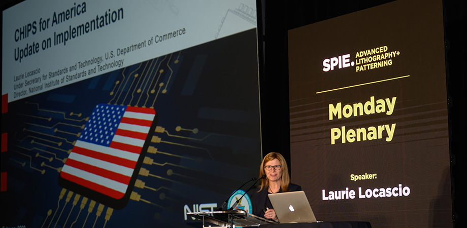
Prior to today's announcement, the National Institute for Standards and Technology (NIST) Director Laurie Locascio opened SPIE Advanced Lithography + Patterning with news that money from the CHIPS for America Act should soon be flowing. To a room full of lithographers, engineers, and chip manufacturers — those best poised to take advantage of the funding — she gave a preview of the announcement and an overview of the implenation plans in her plenary presentation.
“The first notice of funding opportunity, or NOFO, seeks to construct, expand or modernize commercial facilities for leading edge, current generation, and mature nodes,” she said.
Locascio added that this class of possible recipients included facilities for advanced packaging, a vital capability that is absent domestically. This first announcement will be followed by one in late spring aimed at material suppliers and equipment manufacturers. A third funding opportunity announcement will come in early fall to support the construction of semiconductor R&D facilities.
Locascio said that NIST is encouraging all interested parties to submit statements of interest as soon as possible, even if they are a materials supplier, an equipment provider, or only interested in the R&D aspects. In part this is so that NIST can understand needs and by doing so improve the impact of the funding.
“It is critically important we hear from all of you,” she said.
Signed into law in August 2022, the CHIPS for America Act provides funding to the tune of $52 billion to strengthen semiconductor manufacturing in America. Of that, $2 billion goes to the Department of Defense and $50 billion flows through the Commerce Department, with NIST taking the lead. That $50 billion splits into two streams. The bulk of the funds, $39 billion, are for manufacturing support with $11 billion for research and development.
Information is now available at chips.gov, Locascio said. The goal is to invest in projects that meaningfully increase chip production in the United States. In her talk about how to achieve this, Locascio focused on three key pillars: economic resilience and national security, workforce development, and broader impacts.
The first aims to create a safe and secure domestic supply of critical chips. The second and third pillars provide support to do that, while also ensuring that benefits and projects are sustainable environmentally and commercially.

Funding will be in the form of direct investing, loans, or loan guarantees, with one goal being to leverage private money and thereby enhance the investment impact. The application process, Locascio said, involves as many as five steps, with a statement of interest, an optional pre-application, a full application, due diligence on the part of NIST, and then the award presentation. Each deal will be negotiated separately, and NIST has hired a bevy of expert personnel to help it in evaluating proposals and finalizing deals.
On the R&D front, the goal is to address various ecosystem gaps through a National Semiconductor Technology Center, a National Advanced Packaging Manufacturing Program, up to three Manufacturing USA Institutes, and metrology R&D within NIST itself.
In a hypothetical scenario, Locascio said that an auto manufacturer might need advanced semiconductor chips for the development of a self-driving car. It might work through the National Semiconductor Technology Center, which would pull from programs within the Commerce Department or the Department of Defense. The resulting semiconductor technology could be used by defense programs and in the commercial sector, including by the car maker who kicked off the process.
Additionally, Locascio made herself available after her presentation for individuals to ask questions and discuss the funding opportunities for the semiconductor and lithography communities and providing event attendees a chance to get information on NIST's plans firsthand.
| Enjoy this article? Get similar news in your inbox |
|


