A silicon replacement for even smaller transistors?
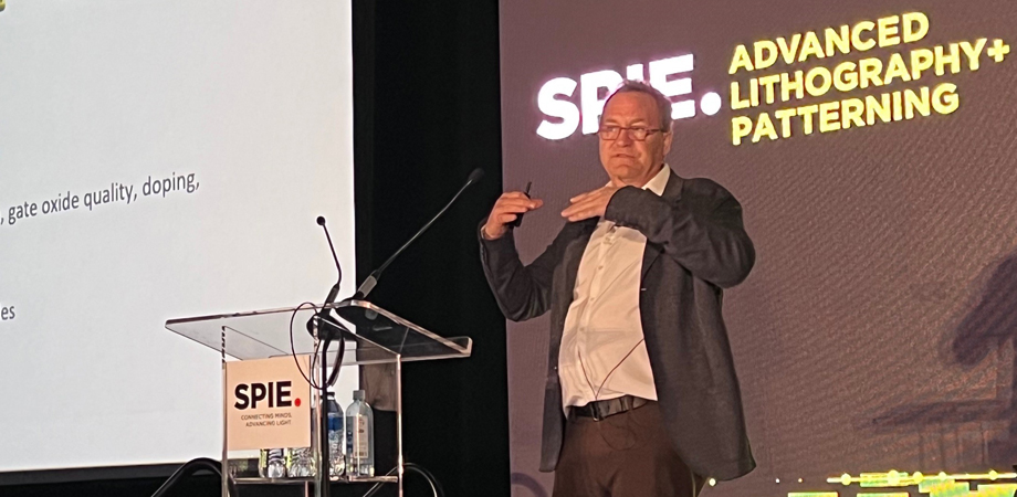
Silicon is the material of choice for computer chips. But problems threaten its dominance for upcoming process nodes, said Kevin O’Brien, an Intel research engineer. In a Tuesday evening presentation at the 2023 Advanced Lithography + Patterning conference, he noted that continued shrinking of transistor cell sizes has a next logical step.
“The natural progression is to just stack them on top of each other,” he said of the transistors in the cell at the beginning of his talk. “That gives you your cell height scaling.”
Silicon, though, has issues when gate lengths get to a few nanometers, which would be the case in this new arrangement. In response, Intel is looking at 2D transition metal dichalcogenides, which consist of a layer of a transition metal like molybdenum or tungsten sandwiched between a layer above and below of a chalcogen atom like sulfur or selenium.
Called 2DTMD, these materials have good electron mobility at nanometer thickness and can be fashioned into transistors that turn on and off, making them potential candidates for tomorrow’s semiconductors. They’re two dimensional in nature because they exist in single layer sheets stacked atop on another. Electrons can’t go either up or down across sheet boundaries, which eliminates scattering issues. From a material standpoint, 2DTMD looks great on paper, O’Brien noted.
But there are major risk areas that need further research and development, he added.
One is simply how to make the stuff. Silicon can be grown into an ingot, which due to research investment can be made to high purity. It’s potential replacement, in contrast, has two possible growth processes: either over a full wafer or selectively from a seed crystal. The former has grain boundary and layer control issues, problems because device materials need to be uniform. The Intel group has demonstrated the feasibility of growing the material selectivity, but more work needs to be done.
Another issue is higher resistance in the contacts, the point at which the material electrically connects with the outside world. If this resistance is too high, then all the benefits of a faster transistor will be lost. A few years ago, contact resistance was at least a factor of 10 higher for 2DTMD than was the case for silicon. Today, O’Brien reported, researchers have closed the gap, with some recent results indicating performance almost on par with silicon.
“We are moving toward silicon,” he said in showing a graph of the latest research.
He noted that these results are not on devices as small as those needed for the next generation of advanced semiconductors. There is a chance that material properties will change when devices of the right dimensions are used, he cautioned. Graphene, a 2D form of carbon, is an example of a material with different properties at nanometer gate widths as compared to those of larger sizes, for example.
A third risk area is etch to remove material. 2DTMD materials are fragile, and so what is needed is a sacrificial layer, something that can be put on top of them to protect them during an etch process. Currently, no sacrificial layer exists.
Other areas that need further research and development involve doping and reliability. Today’s transistors consist of silicon doped as either n- or p-type, with this process creating complementary electrical properties. How to do the same thing to 2DTMD materials is currently a question still to be resolved. The long-term reliability of the new material and devices built from it under the stress of operation and environmental factors like heat and cold is another unknown.
By the end of this talk, O’Brien had gone over quite a list of potential pitfalls. He’d also noted progress, particularly on the contact resistance front, something that members of the audience pointed to in a Q&A after the presentation. The sentiment expressed in relation to contact resistance may best sum up the general impression of the entire talk.
In discussing contact resistance, O’Brien said, “I’m optimistic we can make this thing work.”
| Enjoy this article? Get similar news in your inbox |
|


