Silicon Photonics: Optics’ Next Killer App?
SPIE Fellow and Deputy Director of the University of Southampton's Optoelectronics Research Centre Graham Reed has been working in silicon photonics — pioneering it, in fact — since 1989, when he established the Silicon Research Group at the University of Surrey. So the OPTO 2020 Symposium Co-Chair and Silicon Photonics conference chair at SPIE Photonics West is perfectly placed to eloquently chart the field's exponential growth.
"The focus when I first started working was completely different — low speed, sensor interrogation, sensor chips, stuff like that — but it rapidly changed," says Reed. "Then it looked like conventional optical communications would be the thing, but that transformed into data-com and data centers — that's where the urgent need for low-cost became obvious."
That progress has continued, he notes, particularly in the last decade. "I don't think anyone really expected the silicon modulators to be as good as they are, to go as fast as they do, but things have progressed in such a way that they perform extremely well, and this whole area of photonics has become so much more industrially focused. I mean, if you have a fantastic idea for a new modulator that doubles the speed, everyone's going to be interested, aren't they? But a lot of it is industry taking the research and getting it into a form that's suitable for product and pushing the metrics, making it reliable, getting the yield up, all those things that the academic sector isn't as quick to accomplish."
At the same time, says Reed, multiple new application areas are emerging in silicon photonics. "If you look right across OPTO," he says of one of three symposia at SPIE Photonics West, "LiDAR pops up everywhere - not just in silicon, but in all materials and platforms. So that's booming, and so is imaging in augmented reality, but the latter is really just an application of the former. Also, because of all the advances in silicon photonics, now there's this new whole emerging area of mid-infrared silicon photonics. And sensors are everywhere again, partly because of all the additional on-chip processing you can do, advances in other areas as well as integrated photonics: you can do so much more in integrated photonics as well that now, maybe, all of the potential of a lab on a chip — and systems on a chip, in general — can start to be realized."
In the last five years, Reed says, more and more materials have been integrated on silicon, adding to its functionality. "People think, ‘Well, if you can do germanium maybe you can do III-V compounds on chip. Maybe you can do some fancy electro-optic material for a different type of modulator, or maybe you can have something that you functionalize and have a different type of sensor or other things we just didn't think we could put on a chip.'" Today, he notes, you can make it cheap and disposable and re-useable. "It's wherever your imagination takes you, and it's all merging; the boundaries are disappearing. It isn't just optics either: it's chemistry on a chip, it's biology on a chip, it's more and more electronics."

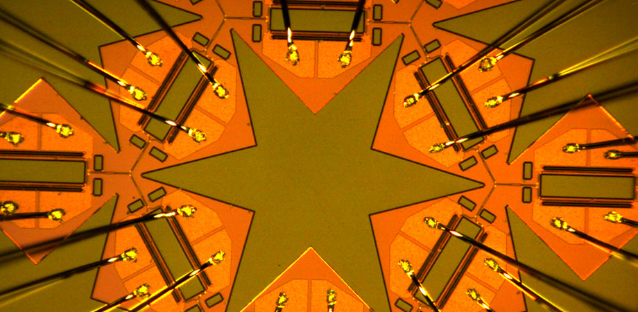
Microscope image of silicon waveguides on a PIC chip which are spiralled up to save space, forming a Mach-Zehnder Interferometer.
Integral to this growing direction, of course, is a much more collaborative approach among scientists, researchers, and engineers. Reed, for example, knows many colleagues working with clinicians on medical applications much earlier in a project's timeline. "They're engaging with these people at the beginning rather than saying, ‘I'll make a sensor then I'll try and sell it to a doctor.' They're thinking a bit more sensibly and engaging the right people to start with. I remember I would try and engage with chemists or biologists years ago, but I didn't understand what they were talking about. They were talking a different language. I didn't understand the words, never mind the acronyms. And for them, it was the same — they didn't know what I was talking about. But if you engage earlier you progress together, you learn each other's languages better, so that process seems like it's changed, it's more collaborative, earlier on."
Collaboration and wider accessibility to silicon photonics are now part of Reed's daily routine. As part of his larger Southampton role, Graham is also the director of CORNERSTONE, a rapid prototyping multi-project wafer (MPW) platform that offers flexible working options to researchers and industry professionals. At the moment, CORNERSTONE offers this service to industry at competitive prices, and to those in UK academics completely free of charge. (The program, in its current iteration, ends in September of 2019).
CORNERSTONE is part of a larger academic-industrial complex that sounds a bit like something out of Wallace & Gromit: the Southampton-based facility is a giant, science-focused sandbox where inventors can play with various materials and innovate to their hearts' content. Traditional foundries are now so much in demand that they've standardized everything, including device-levels, says Reed. It's very difficult, therefore, to be a researcher and go to a traditional foundry: "If you want to try something new, it's hard to do so in that environment."
Under Reed, Southampton created a solution, their own fabrication facility that can fabricate silicon photonics, and integrate with many other unusual materials, or with electronics. Using external foundries can take months to get an outcome, says Reed. "Now, we get an idea, we go downstairs, we try it out, we come back and think, ‘Oh, if we did this maybe it would be better,' and go back and re-work it. You can go around the loop so much more quickly and effectively because you control that fabrication facility. And as a working environment, it's just so buoyant and rich. It's been seven years and I still haven't been into every laboratory — there's a ridiculous number — and then you find out someone else has got a new toy you didn't know about, that can do something else...it's just so conducive to being productive. And it's filled with people who are photonics focused! There are about 350 researchers in the department, so there's lots of people around that know stuff that you don't."

Loading wafers into a furnace tube at the University of Southampton's fabrication facility.
So is silicon photonics the next killer app for optics? According to Reed, it already is. "I would say that was the most notable thing at this year's Photonics West: just a few years ago it was pretty much data-com-focused and now it's pretty much everything. This field's just been blown wide open."
That's quite a panacea for someone for whom developing silicon photonics hasn't been completely smooth sailing. Back in the 90s, he was working closely with Bookham Technology, the first Silicon-Photonics company in the world — at that time, in fact, the only one — which happened to have been founded by one of Reed's former students, Andrew Rickman. "At one point," says Reed, "Bookham decided to get out of silicon and I thought, ‘Uh oh!' — I really thought it might be the end of silicon photonics, and that I was going to have to do something else with my career."
Two weeks later though, Intel came calling, looking for a consultant in silicon photonics. "And, of course, once someone like Intel gets involved then so does IBM and all the other big boys. That was the beginning of the explosion, really," says Reed. "When Intel announced their first one-gigahertz modulator, I'd been working with them for two years. So you do get these cycles." Reed pauses. "Actually," he says, "in the case of silicon photonics it's been more like a massive up-wave."
| Enjoy this article? Get similar news in your inbox |
|