Optical lithography is limited by diffraction, which is most significant when objects are comparable in size to the wavelength of light. This fact of physics has driven decreases in the wavelength of light used in optical lithography. Similarly, the use for lithography of wavelengths in the x-ray portion of the electromagnetic spectrum was motivated by the idea that diffraction effects could be effectively neutralized by using photons with extremely short wavelengths. However, at x-ray wavelengths there are no known materials for making image-forming lenses or mirrors. Consequently, x-ray lithography involves the use of proximity printing, where the mask is brought to within a few microns of the wafer and the x rays are passed directly through the mask and onto the wafer (Fig. 12.1). This is in contrast to optical lithography, which has the potential for projection of the image by a lens.

Since there are no materials that are highly transparent, x-ray masks are comprised of very thin membranes (thickness < 2 μm) comprised of low-atomic-number materials, on which the circuit patterns are placed in the form of high-atomic-number material (Fig. 12.1). A large percentage of the x rays pass through the low-atomic-number material, but the x rays are generally absorbed or scattered by the high-atomic-number materials, thus generating a pattern contrast. Silicon carbide is a typical membrane material, and silicon nitride films were used early in the development of x-ray lithography.
Silicon carbide is a good material to use for the membrane because it has a high Young’s modulus (450 GPa), a characteristic that minimizes mechanical distortion, and it is not damaged by long exposure to x rays.1 Gold2 and tungsten3 have been used as absorbers, but the best success has been found with compounds of Ta, such as TaN,4 TaSiNx,5 and Ta4B,6 because they are compatible with various etch and cleaning processes.7
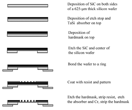
The use of thin membranes for masks introduces a set of challenges. Such films deform because of stresses, and there has been extensive work to understand and control them.8,9 Mask deformation is particularly problematic for x-ray lithography, because there is no reduction of the image between the mask and wafer. This 1:1 pattern transfer necessitates very tight tolerances for the masks, relative to 4:1 or 5:1 reduction printing. On the other hand, with x rays there are no lens distortions or feature-size-dependent pattern-placement errors, so a greater part of the overlay budget can be allocated to the mask in x-ray lithography. However, thin-film masks are susceptible to vibrations when stepped or scanned, and this needs to be addressed in any x-ray exposure system.10 Diamond is being pursued as an x-ray-mask-membrane material because its extremely high Young’s modulus (900 GPa) reduces mask mechanical distortion.11 X-ray masks are typically made from silicon wafers. The membrane-mask area is fabricated in the center of the wafer. The mask fabrication process is outlined in Fig. 12.2. Because the membrane area is fragile, and silicon wafers are too thin to provide stability, frames or rings have been adopted for x-ray masks, although a standard for such frames has not reached an industry-wide consensus. The fragile silicon wafer is bonded to the ring to provide mechanical strength. An example of such a frame, the ARPA-NIST standard,12 is shown in Fig. 12.3. The frame is made of Pyrex to facilitate bonding between the frame and the silicon on which the mask is fabricated.
There has been greater investment in x-ray lithography than any other potential successor to optical technology. There have been programs at several universities, such as MIT and the University of Wisconsin, and at companies such as IBM, AT&T, and NTT. X-ray technology has also received support from the US and Japanese governments. X-ray step-and-repeat and step-and-scan systems were made available commercially.13,14

References
- P.A. Seese, K.D. Cummings, D.J. Resnik, A.W. Yanfo, W.A. Johnson, G.M. Wells, and J.P. Wallace “Accelerated radiation damage testing of xray mask membrane materials,” Proc. SPIE 1924, pp. 457–466 (1993).
- G.E. Georgiou, C.A. Jankowski, and T A. Palumbo, Proc. SPIE 471, pp. 96 (1984).
- K.D. Cummings, D.J. Resnick, J. Frackoviak, R.R. Kola, L.E. Trimble, B. Grant, S. Silverman, L. Haas, and B. Jennings, “Study of electron beam patterning of resist on tungsten x-ray masks,” J. Vac. Sci. Technol. B 11(6), pp. 2872–2875 (1993).
- J.T. Sheu, A. Chu, J.H. Ding, and S. Su, “Characteristics of sputtered TaX absorbers for x-ray masks,” Proc. SPIE 3676, pp. 42–45 (1999).
- J.M. Rocque, D.M. Puisto, D.J. Resnick, K.D. Cummings, W. Chuc and P.A. Seese, “SNR200 chemically amplified resist optimization,” Proc. SPIE 3048, pp. 90–99 (1997).
- C.J. Brooks, K.C. Racette, M.J. Lercel, L.A. Powers, and D.E. Benoit, “Advanced refractory-metal and process technology for the fabrication of x-ray masks,” Proc. SPIE 3676, 14–23 (1999).
- J. Leavey and P.J.S. Mangat, “Mask and wafer inspection and cleaning for proximity x-ray lithography,” Proc. SPIE 3331, pp. 179–188 (1998).
- E.P. Cotte, R.L. Engelstad, E.G. Lovell, and C.J. Brooks, “Predicting mechanical distortions in x-ray masks,” Proc. SPIE 3676, pp. 429–440 (1999).
- M.F. Laudon, D.L. Laird, R.L. Engelstad and R. Cerrina. “Mechanical response of x-ray masks,” Jpn. J. Appl. Phys. 32, pp. 5928–5932 (1993).
- M.P. Schlax, R.L. Engelstad, and E.G. Lovell, “Dynamic characterization of step-induced vibrations of x-ray mask membranes,” Proc. SPIE 3331, pp. 629–637 (1998).
- C.J. Brooks, L.A. Powers, R.E. Acosta, D. Molly, F. Faili, and J.A. Herb “Characteristics of chemical vapor deposition diamond films for x-ray mask substrates,” J. Vac. Sci. Technol. B 17(6), pp. 3144–3148 (1999).
- D. Laird, M. Laudon, and R. Engelstad, “Practical considerations in x-ray mask mounting methodology,” J. Vac. Sci. Technol. B 11(6), pp. 2953– 2957 (1993).
- K. Uda, N. Mizusawa, Y. Tanaka, Y. Watanabe, H. Ina, and S. Uzawa, “X-ray stepper development for volume production at Canon,” Proc. SPIE 3331, pp. 689–697 (1998).
- Q. Leonard, J. Wallace, O. Vladimirsky, K. Simon and F. Cerrina, “X-ray mask replication using a Suss stepper at CXrL,” Proc. SPIE 3048, pp. 299–303 (1997).
H. J. Levinson, Principles of Lithography, Second Edition, SPIE Press, Bellingham, WA (2005).
View SPIE terms of use.