OPTO Plenary Likes Facebook's Schmidtke
The OPTO plenary session highlighted the emerging power of deep learning in microscopy and imaging, the advent and continued promise of photonic crystals, and the need for new photonics technology to handle increasingly large-scale data networks
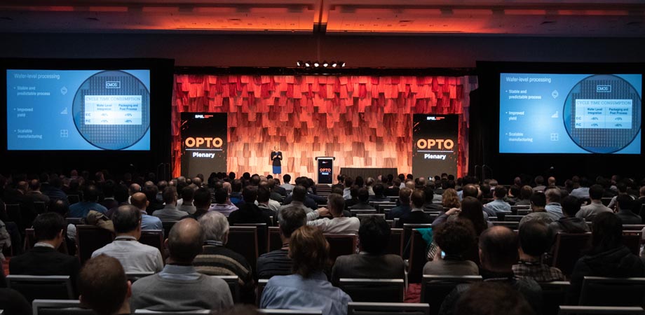
For companies like Facebook, which has submarine and long-haul networks, the demand on their data infrastructure is putting stress on available technology. "The amount of data we have at the data center and the speed at which we need to move it around has developed so quickly it's outpaced the rate of innovation in the rest of the market," Katharine Schmidtke, who leads optical technology strategy at Facebook, told the Show Daily.
While internet traffic is always growing, machine-to-machine traffic is exploding even faster, due to the need to back up data, and for optimization.
The data centers themselves are enormous, she said. Facebook's Altoona data center in Iowa, for example, is equivalent in size to the Empire State Building on its side. As much optical fiber is inside these centers - tens of thousands of kilometers in total length - as there are outside, connecting the centers.
To handle rising data demand, these hyperscale data centers require new photonic technology, Schmidtke said. For its part, Facebook is trying to influence and inspire what comes next.")
There is a particular need to accelerate the rate of data transmission while maintaining power efficiency. For example, data centers will need integrated switch ASICs, the hubs that control the networks connecting the servers. Such devices now consist of separate modules, but if they were integrated into a co-packaged unit, they would allow for higher data rates and save power.
Another need is to incorporate more automation in manufacturing. She envisions that one day, photonic circuits can be printed using methods similar to CMOS technology.
Reviewing 20 years of development, Susumu Noda of Kyoto University highlighted the promise of photonic crystals, which have potential applications in areas such as quantum information processing, laser technology, and the new field of topological photonics.
"Photonic crystals could be one of the most important materials in the 21st century," Noda told Show Daily.
In 1999, Noda and his colleagues used a water fusion technique to develop the first complete 3D photonic crystal that worked in optical wavelengths. By stacking crisscrossing bars of gallium arsenide on top of each other, they built a nanoscale 3D photonic crystal that bottles up photons of a certain frequency - a so-called complete photonic crystal.
In 2000, Noda and colleagues developed the first 2D photonic crystals, thin semiconductor sheets covered with holes. Depending on the hole pattern, the sheets can trap and channel light. A small area without holes can form a nanocavity that traps photons. Such nanocavities can be embedded with quantum dots to serve as quantum bits and a platform for quantum information processing. 
Shifting the spacing between the holes by just a few to tens of nanometers prevents these cavities from leaking photons, thus increasing the Q factor by as much as 10 million times, Noda said.
One of the most important applications of photonic crystals is in semiconductor lasers, he said. While their compactness remains an advantage, today's semiconductor laser beams can degrade rapidly, limiting their power output to just a tenth of carbon dioxide, disk, or fiber lasers.
But as Noda has shown, 2D photonic crystals can enable semiconductor lasers that are bright and narrow without the need for collimating lenses. These lasers would be useful for manufacturing and processing materials and for LiDAR technology, which are crucial for technologies like autonomous vehicles.
Using photonic crystals, Noda has also demonstrated how to control thermal emission, converting a broad spectrum into a narrow one without the loss of energy. The researchers can also switch the emission on and off, creating an efficient infrared light source for environmental and biological sensors.
These types of technologies will be essential for a future society in which cyberspace is integrated with physical space, he said.
Concluding the session was Aydogan Ozcan of the University of California, Los Angeles, who described how deep learning techniques are changing imaging and microscopy.
"Deep learning and neural networks are helping us create new types of imaging and sensing systems that are fundamentally more powerful and work differently from traditional, physics-based solutions," he told Show Daily.
The idea is to apply these computational techniques to process the image as it's being taken in real-time. Such techniques, for example, can be used to identify objects immediately, as they are being imaged.
With conventional image-recognition methods, a system takes an image and then processes it after the fact. Ozcan's group has built a device consisting of several layers of polymer wafers that diffract the light coming from an object. Using a so-called diffractive neural network, the system can identify the object - handwritten numbers and clothing, in their experiment - by measuring where most of the light leaves the wafers.
The researchers have also used deep learning techniques to reconstruct holograms out of 2D images - a much faster and powerful process than conventional holographic techniques. They used their method to make holograms of Pap smears, but it would be powerful in all areas of medicine.
Most recently, the researchers used deep learning techniques to effectively turn a low-resolution microscope into a super-resolution one. They previously did similar work to enhance cell-phone images of biological samples to match those taken with laboratory microscopes.
By incorporating computational analysis and statistical learning into the front-end of an imaging technique, the researchers are creating an approach to imaging that doesn't just passively collect light. "We can essentially create thinking microscopes," Ozcan said.
-Marcus Woo is a freelance science journalist based in California. A version of this article appeared in the Photonics West Show Daily.
Related SPIE content:
See the OPTO presentations from SPIE Photonics West 2019.
Facebook focuses on optics integration
| Enjoy this article? Get similar news in your inbox |
|


