Hiroo Kinoshita: Lighting the way for extreme ultraviolet lithography
The idea of extreme ultraviolet lithography (EUVL) came to Hiroo Kinoshita while he worked for Nippon Telegraph and Telephone (NTT) in the mid-1980s—a time when semiconductor lithography still depended on mercury lamps. The semiconductor industry wanted shorter wavelengths for lithography to sustain Moore’s law and continue increasing the number of transistors on a chip that was powering industry growth. Ultraviolet lithography with excimer lasers was already in the pipeline. Kinoshita was looking to much shorter X-ray wavelengths, but kept finding daunting problems, including a lack of lenses or mirrors capable of focusing X-rays for lithography.
Then he came across a paper by Jim Underwood and Troy Barbee, reporting the first multilayer mirrors for wavelengths of 10 to 100 nm that we now call EUV. That was a huge advance over the glancing-angle reflectors that at the time were the only mirrors available for X-rays at shorter wavelengths. Kinoshita realized that the new mirrors could open the door to lithography at EUV wavelengths. In fact, he tested them and succeeded in demonstrating the first focusing of images in the EUV and reported his achievement at a 1986 meeting of the Japan Society of Applied Physics.
Kinoshita was ahead of his time. “Unfortunately, the audience was highly skeptical of my talk,” he said later in an invited lecture on the emergence of EUV lithography. “However, my belief did not change.” He continued pursuing EUV lithography and is recognized today as its founding luminary. Nonetheless, overcoming the formidable challenges required more than 30 years of effort, billions of dollars in funding, and a cast of thousands of engineers and scientists.
Developing a suitable EUV light source was one of the most obvious and difficult challenges. In the mid-1980s, Obert Wood and Bill Silfvast at Bell Labs tried to develop one based on emission from a laser-produced sodium plasma. They found it easier to study how it would work by using a synchrotron to generate light in the 10 to 100 nm range, then called soft X-rays.
“The synchrotron did not supply much power, but its output could be adjusted to match reflective coatings on the imaging mirrors,” says Wood. Others were skeptical. Then, around 1993, one of their managers, Rick Freeman, recommended a name change for the technology: “extreme ultraviolet lithography, which sounds like deep ultraviolet lithography,” which was already being done with excimer lasers, Wood recalls. “People immediately jumped on that.”

Meanwhile Kinoshita continued his efforts with a group of about five others.
NTT was more interested in other types of lithography, but he credits them with not stopping his research. In 1993, he organized a US-Japan meeting on EUV lithography that attracted about 50 researchers and built a bond between the two countries.
By then, “Moore’s law was in trouble,” says David Attwood of Lawrence Berkeley National Laboratory (Berkeley Lab). The 193 nm argon-fluoride laser was already in development for photolithography, but that was looking like the end of the road for lithography with deep-UV lasers. Having no way to continue shrinking chip geometry would have been a very big problem for Intel, “which counted on being at the forefront of Moore’s law to sell its products at high prices.” In fact, the whole community was growing very anxious about the future.
Attwood says the turning point came when Intel Research Director John Carruthers took a long hard look at future options and concluded that the only viable course for the company was to place a billion-dollar bet on an industry-wide project to develop a new technology for EUV lithography. When he proposed the option to his bosses, Andy Grove pounded the table in anger, but Gordon Moore didn’t see an alternative and, in the end, Grove went along. Moore further backed Carruthers’ effort to enlist other companies by announcing at an industry meeting, “Intel is here…we are placing our bet and we want you to join us.”
Intel’s call to action succeeded. In 1997, long-time industry competitors, recognizing the severity of the threat, joined together to incorporate Extreme Ultraviolet LLC to develop a new generation of lithography. The consortium contracted with the US Department of Energy to organize research at Berkeley Lab, along with Lawrence Livermore and Sandia National Laboratories. Attwood, who headed Berkeley Lab’s EUV research, recalls the atmosphere as collegial, and counts many EUV LLC colleagues as fast friends. Japan formed a similar group, EUVA, which cooperated with EUV LLC. Wood has fond memories of Kinoshita taking him on a tour of the centuries-old Himeji castle in Japan.
The consortium members’ task was huge. Moving lithography to the EUV required not just new sources, but new optics and optical coatings, photoresists, measurement tools, and nanometer-scale precision. They started with six candidate approaches and gathered every six months to rate them and compare results. Over time, and after several iterations, their research changed their minds, and the laser-produced tin plasma source initially rated last became the top choice.
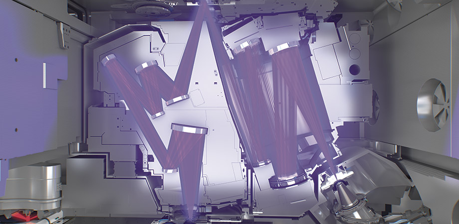
Optical requirements were especially stringent. A dozen separate mirrors were needed to project the image of the circuit mask onto the silicon surface with the required nanometer resolution. The only option in the EUV was multilayer mirrors, which had quarter-wave layers thinner than 4 nm that had to be kept uniform to daunting accuracy. With maximum EUV reflectivity, after a dozen reflections from a 70 percent reflective mirror, you wind up with about 1.4 percent of the light left. The 13.5 nm source wavelength used was chosen because it was the peak reflectivity of mirrors made of stacks of molybdenum disilicide and silicon.
By the mid-2000s, researchers had demonstrated tin-plasma sources pumped by carbon dioxide lasers, but their power was limited. Improvements were painfully slow, with output stuck in the watt range for several years. Signs of progress emerged in 2013, when California company Cymer reported pushing EUV power above 10 watts by hitting the tin with a pre-pulse before the main one. That was far short of production requirements, but ASML in The Netherlands, which at the time produced two-thirds of chip production machines, bought Cymer in May of that year, and started pumping money into scaling EUV lithography.
By then, ASML in partnership with Zeiss had spent 20 years developing the complex optics needed for EUV lithography. “It was really a huge amount of work to turn the [patent] concept into a reality,” says Erik Loopstra, who with Vadim Banine, led the partnership’s research team. Freeform optics focuses the EUV light along a 10 m optical path and down to a nanometer- scale spot. “It’s like hitting a golf ball on the moon,” he says. “Measurement is the key to getting it done. Everything you can measure, you can manufacture.”
Today, ASML is the only company selling EUV fab machines, each one slightly smaller than a bus and costing $150 million. Together with Zeiss, it has 2,500 people building the fabs. The illuminators alone have 15,000 parts, with another 20,000 in the projection optics. Loopstra says it’s more complex than the space shuttle. And they’re already working on the next generation, which will increase numerical aperture from 0.33 to 0.55, allowing focus down to an even smaller spot than today’s capability.
Kinoshita, now a professor at the University of Hyogo in Japan, says EUV lithography “was my dream.” He had expected development to take a long time, and says he is “so happy” today to see it realized.
Jeff Hecht is an SPIE Member and freelancer who writes about science
and technology.
| Enjoy this article? Get similar news in your inbox |
|


