Editor's desk: Light is at the heart of it
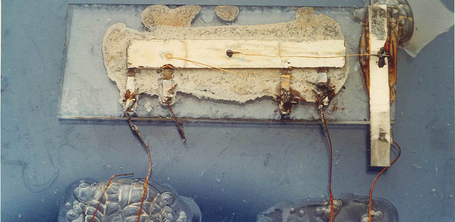
In 1958—the same year Charles Townes conceived of the optical maser—Jack Kilby created the first integrated circuit on a slab of germanium. It had wires hanging off the side, and looked a bit like a kid's first attempt at welding in shop class, but it was a major step forward in proof of concept. Meanwhile, at Fairchild Semiconductor, Robert Noyce was working with the Fairchild Eight—also known as the Traitorous Eight (cue ominous music)—to develop a planar integrated chip on silicon. His method proved scalable, and quickly moved to manufacturing.
In 1960, Texas Instruments sold their first chip, the "502 Flip Flop," for $450. It had one bit of memory. Since then, chip manufacturing has scaled in every way so that a modern microchip costs mere picocents per bit.
While the cost to make a chip has fallen over the past 60 years, our reliance on computer chips costs in other ways. Data centers use enormous amounts of energy to power their servers and store our information. Chip fabs consume city-sized amounts of electricity and water. And our myriad electronic devices, from phones to laptops to Fitbits, often reach obsolescence after just three to four years. Millions of devices end up in landfills each year, along with the copper, silver, and rare earth metals they contain.
Fortunately, many people working in photonics are looking for solutions. Some researchers want to improve the efficiency of computing by rethinking the very foundation of computational architecture. Neuromorphic design attempts to mimic the speed, flexibility, and efficiency of the human brain by reproducing its structural elements in hardware. More traditionally, chip fabs are trying to green their technology through renewable energy and recycled water.
Today's most advanced chips are created using a process called EUV lithography, and at the heart of EUVL is a CO2 laser. In fact, photonics—and lasers in particular—are at the heart of many modern manufacturing processes. Sure, there are the obvious industrial uses, like laser cutting and welding. But photonics has a role in manufacturing in unexpected ways, too, like the Advanced Photon Source at Argonne National Laboratory, where researchers pummel materials with photons to test their response to extreme stress and find nanoscale weaknesses before they become problems.
This issue of Photonics Focus explores the tools at the heart of modern commerce, from the wonderous chip, which has doubled the density of transistors in a circuit every few years as it inches toward the conclusion of Moore's law, to advanced laser technology.
1958 was a big year for photonics. It set the stage for the foundations of modern industry.
Gwen Weerts, Managing Editor, Photonics Focus


