Guiding light without glass
For millennia, optical lenses have been smooth, curved, and made of glass.
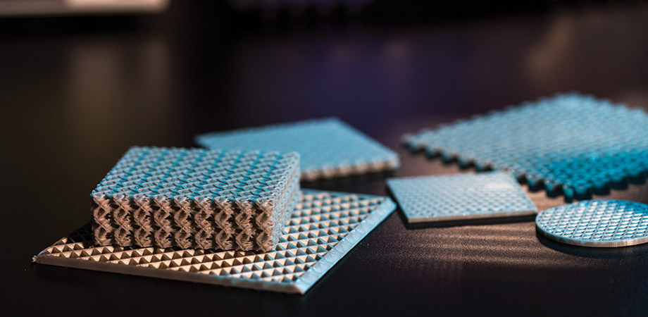
But in 2016, Frederico Capasso at Harvard University made a lens that was none of these. Seen with a microscope, his "lens" looked more like an army of dominoes assembling for war.
In fact, each of these dominos was a 600 × 400 × 85 nanometer pillar made from titanium dioxide—called a nanofin because of its notched shape—arranged on a silicon dioxide wafer. Together, they formed one of the thinnest and flattest lenses ever created, with an optical resolution that put many commercial lenses to shame.
The nanofin works because light is diffracted by structures that are roughly the same size as its wavelength. What's more, such diffracted light waves will interfere with one another, leading to bright and dark splotches.
A material that interacts with light through geometry rather than chemistry is called a metamaterial. If the geometry is restricted to a surface—say through many light altering notches such as a nanofin—the surface is called a metasurface.
Capasso demonstrated that if these structures were carefully arranged and meticulously fabricated, they could actively engineer a wavefront. They could, for example, conform light to a tight focus making a lens, or split white light into several colors creating a spectrograph.
Today, the field of metamaterials is moving forward rapidly thanks to a bunch of pioneers and their bold algorithms. Increasingly, the designs are being generated by artificial intelligence using human prompts. That's because we don't really know how to go from a proposed application—such as a lens—to a design that works for it. In addition, metamaterials are complicated structures that we are just getting to know.

The nanofins on a metalens surface. Each nanofin is made from titanium dioxide and is 600 nm high. Courtesy of Federico Capasso
"These are a class of materials where you create nonconventional electromagnetic, photonic, or acoustic properties that do not exist in conventional bulk materials through engineered subwavelength features," explains Ali Adibi, professor of photonics at Georgia Tech.
"Optics is usually glass," says Ravi Hedge, professor at the Indian Institute of Technology, Gandhinagar. "Metamaterials enable new kinds of devices without using glass, that don't rely on curvature [to guide light], but nanostructures."
Metamaterials devices promise a broad range of revolutionary applications. They could be used to create flat lenses necessary for miniaturizing cell phones, microspectrographs that could reveal the presence of toxic metals and other chemicals in a volume, components for quantum computers, cryptography and security, digital electronics that rely on light instead of electrons, and cloaking materials that render objects invisible.
Since structure is more important for these materials than chemistry, most of them are made with silicon and other conventional electronic materials that we know very well how to etch intricate structures on using established processes. This has made meta-materials attractive to many device manufacturers, and metamaterials research is one of the hottest topics in science.
The number of possible metamaterials is infinite. You can craft any number of structures—pillars, bars, rods, spheres—on the nanoscale, and arrange them in any combination. Each design element can be made of slightly different dimensions and of different materials. They can be stacked, rotated, or made to intersect. Each structure has a unique electromagnetic response that can be precisely calculated.
But the reverse problem—calculating a design that gives the desired performance—turns out to be extremely challenging.
"Designing custom metamaterials is challenging because each device has many dimensions, and each dimension can have tens to hundreds of parameters," says Jonathan Fan, a professor of electrical engineering at Stanford University. Suppose a device has 10 free parameters that can be altered, and that each of these parameters, called dimensions or degrees of freedom, can take any of 10 possible values. That gives a total of 1010 structural choices—an impossibly vast space to explore.
Many commercially available software packages can calculate the electromagnetic (EM) output response (also known as EM solvers) for a given input structure and incoming light wavefront. They rely on Maxwell's Equations, and are highly accurate, but tend to be time consuming.
"Suppose each calculation requires five minutes," says Adibi. "It would take 5 × 10¹⁰ minutes to check the whole design space." That's roughly 95,000 years.
One approach, then, is to use mathematical techniques to reduce the number of dimensions of the problem. "All we are doing is intelligent search," explains Adibi. Recently, he used such a method to design a reconfigurable metamaterial that changes shape when an electric field is applied. These designs can play an active role in devices, instead of the passive designs currently being explored. However, dimensionality reduction is not always a solution because the time required for the reduced dimensions can still be enormous.
That's why metamaterial researchers are increasingly turning to data-driven approaches such as deep learning to tackle the inverse design challenge.
In this approach, small computational elements called neurons store two numbers called weight and bias. An input signal is multiplied by the weight and added to the bias. If it exceeds a certain threshold value, the neuron passes the signal to the next neuron it's connected to where the whole process repeats with a different weight and bias. Typical deep learning architectures used in language and image processing contain billions of these neurons each with a weight and bias.
The power of deep-learning models is that they can learn the correct weight and biases for an application from examples. For instance, a sequence of metamaterial designs and their outputs can be fed to a neural network. The model's output is compared to a regular EM solver and the result is fed back into the network. Over hundreds and thousands of examples, the deep-learning model twiddles its weight and biases until the output matches what was calculated using Maxwell's equations. Once the model is trained, the neural network can calculate a response in a matter of seconds.
If this sounds really complex, it is. But it has been shown to work again and again for all sorts of applications ranging from self-driving cars and language translation, to image recognition.
No one really knows how neural networks are able to learn so well. A leading theory is that they act as sieves for data, so that only the most common—and hence fundamental—pieces of information reach the other end. Because they are modeled on the human brain, this paradigm is known as artificial intelligence (AI).
Hedge uses this approach in conjunction with a so-called evolutionary algorithm to calculate the best designs for a metamaterial color filter and color splitter.
"A color filter separates out a particular color from white light. A color splitter will separate out wavelengths of light like a prism and direct each color in a different direction," he says. It could be useful, for example, in some types of solar cells where infrared, ultraviolet, and visible light can be used simultaneously.
Hedge first trains a neural network to learn the electromagnetic response of metamaterial structures from hundreds of examples. This deep learning model does what an EM solver does but in a fraction of the time. A set of randomly generated designs are checked with the model, following which the poorest designs are dropped. The remaining designs are tweaked and made to swap design elements with other structures. This imitates a computerized version of evolution and natural selection with the Darwinian goal of surviving the chopping block at the model. During thousands of such iterations, the model continually improves its performance to reach an optimal design.
While evolutionary approaches are powerful and effective, deep learning can also be used directly for inverse design.
At Northeastern University, associate professor of electrical and computer engineering Liu Yongmin creates chiral metamaterials that separate light according to its polarization. Chirality refers to the handedness of a molecule. DNA, for example, is right-handed, like most molecules in the human body. "Polarized light interacts with chiral molecules differently and can be used for medical diagnostic and analytic purposes," he says.
Yongmin uses specialized deep learning architectures to solve the inverse design problem. In one, called an autoencoder, the input structures and their EM responses are used by a neural network to learn a mathematical representation called a latent space, which is like a map of the design space. If a good design is located at one point of the latent space, nearby points must also be good. New metamaterials can be designed easily once the latent space has been generated. Yongmin has used this method to generate new chiral metamaterials as well as information storage devices.
Though impressive, deep learning cannot guarantee the perfect metamaterial design for a given application. That's because the inverse design problem does not always have a unique solution. Multiple structures that are not identical can produce the same output response. So, it's possible that a design discovered using hours of laborious computation might not be the best device in terms of performance or the easiest to manufacture.
To understand why this might be the case, we need to imagine that every possible design—excellent, good, bad, and terrible—is placed on an imaginary landscape such that the elevation of each device is inversely proportional to its performance. The best solutions—devices that meet our criteria—are the ones that lie at the bottom of a pit. Translated into this landscape, the goal of the inverse design problem is to find the lowest point starting from some random location.
The problems that deep learning excels at solving have simple bowl-shaped landscapes with a clearly defined lowest point. The metamaterial design landscape, on the other hand, is more like the Appalachian Mountains with many peaks, valleys, crevices, and chasms. Each chasm gives us a device that produces the desired response, but there is no guarantee that we have reached the deepest point, or correspondingly, the best possible device.
At Stanford, Fan is pioneering a method that tackles this problem head on. Called GLOnets (global topology optimization networks), his approach uses neural networks to smooth out the mountainous landscapes of other neural networks. Fan's group has used this method to design high-efficiency diffraction gratings and thin-film stacks.
He is also working towards making the neural networks physics aware. The idea is to incorporate physical equations—such as the wave equation—into the training for deep learning models so that their efficiency and performance can be further fine-tuned.
Fan advocates Metanet, an open database where anyone can upload and download metamaterial designs and their resulting responses. His vision is to have a platform that allows anyone to check or validate an idea for a design within a few seconds or minutes of conception. This will enable everyone to have access to plentiful training data for their models, in addition to the trained models.
"In the metamaterial community, it is difficult to compare algorithms as everyone solves their own problems. Without a standardized dataset, it is difficult to compare results and to coordinate research efforts," he says. This sentiment carries across the community.
"We should share data," Adibi says. He proposes that companies that develop commercial photonics software provide a common platform for data sharing.
The other crux in the community is being able to learn new physics from the models generated by deep learning. Neural networks are considered something of a black box, meaning that there is often no explanation for how the model arrived at a particular solution other than through laborious number crunching. As a result, the photonics community doesn't learn anything new, even if all the inverse design problems have been solved. Only genuine scientific insights might advance metamaterials to the next stage in their evolution.
For example, the design elements of a successful model could be performing novel nonlocal interactions that could help in engineering better devices. "Explainable AI is necessary to tackle even more complex problems, such as heterogeneous metamaterials," says Hedge. These are made from multiple materials and span a wider range of chemistries than the systems studied today. Their potential applications are also consequently more diverse.
"The whole relationship between inputs and out-puts is in the neural network weights," notes Adibi. "If you try to understand them, they may tell a lot about a hidden world we don't understand well."
Vineeth Venugopal is a science writer and metamaterials researcher who loves all things and their stories.
| Enjoy this article? Get similar news in your inbox |
|


