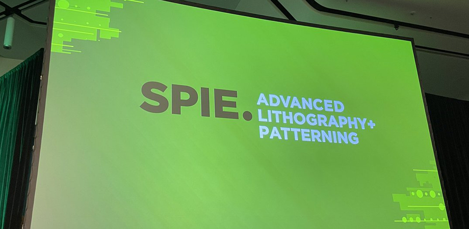
Reflecting its importance, the next generation of EUV lithography, high-NA EUV, appeared in multiple presentations every day of the 2022 SPIE Advanced Lithography and Patterning conference. Three samples illustrate the breadth of efforts to bring the latest EUV technology into high volume production.
On Wednesday, in the first example, Timothée Allenet, a researcher at the Paul Scherrer Institut in Switzerland, reported results from an EUV resist screening program. In photolithography, photons strike resist and alter it, thereby transferring a mask pattern to a thin resist film on a wafer. A resist’s ability to perform this task is critical to making a chip.
But in testing and evaluating a resist, researchers face a problem. High-NA EUV scanners aren’t readily available, yet they’re needed for resist development. So Allenet and his fellow researchers came up with a suitable substitute, using a beamline from the Swiss Light Source (SLS) at the Paul Scherrer Institut. This gives them access to photons that closely approximate what an EUV scanner uses and the ability, when used with a simple mask, to produce periodic lines and spaces as well a regular array of holes.
The test conditions aren’t the same as actual production. However, they meet the researchers needs.
“We’re here to do preliminary testing,” Allenet said of the program done in collaboration with EUV scanner maker ASML.
The results in Allenet’s presentation indicate that chemically amplified resists, the workhorse technology of the industry for decades, may be on the way out. Metallic oxide resists, at the moment, offer the ability to resolve smaller features, which is the whole point of moving to high-NA EUV. Allenet noted, though, that these findings are not from a next generation EUV scanner, and so it’s unclear exactly how, or even if, the better resist performance will translate when run on actual product.
On Thursday, in a second example, Angélique Raley, an etch process manager and technical staff member at Tokyo Electron Center of America, reported on a holistic approach to patterning. In semiconductor processing, after resist patterning a follow-on process etches that pattern into the chip layer below. In this way, an intended feature eventually ends up on the wafer.
In the process, lithographers face what is known as resolution, line width roughness, and sensitivity tradeoff. The three interact, and better resolution means rougher lines and smoother lines result in worse resolution. Clever etch processing, though, can help.
“The RLS tradeoff is very much a focus of ours,” Raley said. “Being able to reduce the dose while maintaining roughness is the key to ensure that EUV manufacturing is cost effective.”
She noted that high-NA EUV has a shallower depth of focus, which means resist layers must be thinner. However, most etch processes remove resist. Thinner resist can thus present problems.
After noting that the initial resist choice is critical to success, Raley went over results that showed that process adjustments, such as the use of selective deposition in an etch chamber, can help. Selective deposition adds material to the resist but only in specific areas. If done in the right way, this allows processing thinner resist.
In a third and final example, a presentation on Wednesday explored lithography simulation. There are many possible chemical formulations for resists. So, how do researchers narrow down the field and pick which one or ones to concentrate on?
One solution is to do simulations, thereby trying out various possibilities in a computer. Patrick Theofanis, a senior software engineer at Intel, spoke about the Monte Carlo EUV stochastic simulator – MESS for short.
“The simulator is based on fundamental chemistry and fundamental physics,” Theofanis said.
The simulator aims to speed up the pace of resist development by helping researchers narrow their focus more quickly through rapid elimination of poor formulations. Another goal of the simulator is to provide predictions about how resists perform in high-NA EUV lithography. A third objective is to help explore stochastic, or random, defect causes to help produce better design rules.
The simulator gives good agreement with real-world measurements, matching them to within a few percent. It can tell a good resist from a not-so-good one, Theofanis said. As for the stochastic defects that trouble EUV, simulations suggest these might start with a lack of photoionization of the resist, a thin spot in the resist, or another small problem. That starts a failure chain that creates a defect.
In summing up this part of what the simulator offers, Theofanis said, “It provides us an enormous amount of data, and with that data we can do a root cause of analysis of stochastic defects.”
Hank Hogan is a science writer based in Reno, Nevada.
| Enjoy this article? Get similar news in your inbox |
|


