New Use and Challenges for a Mature Technology

There may be a new use for old lithography technology, according to presentations at the February 2020 SPIE Advanced Lithography conference. Old is relative, as in this case the lithography is the optical variety still widely used in semiconductor fabrication.
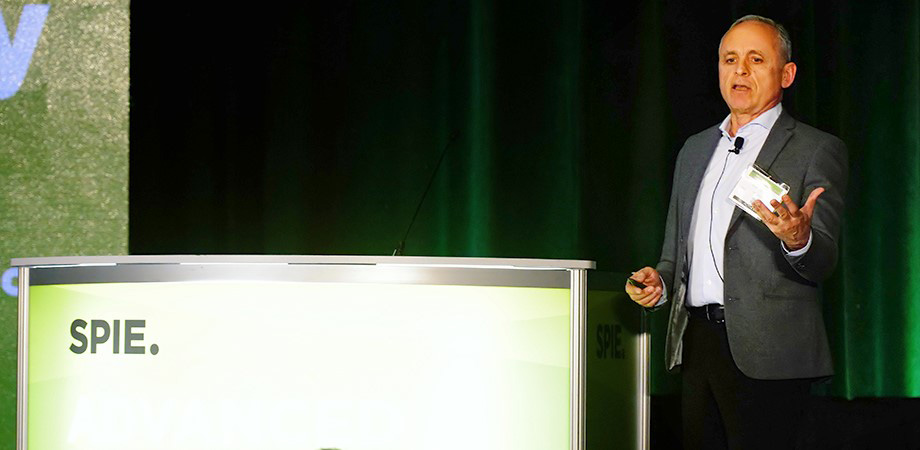
The use, on the other hand, is really new, a fundamental shift in computing driven by the needs of artificial intelligence or AI. The reasons for this were outlined in a plenary talk from Evangelos Eleftheriou, an IBM Fellow who focuses on cloud and computing infrastructure.
He noted that neural network-based deep learning has achieved human-like performance in classifying objects. Show a person and an AI system pictures of cats, say, and the two do an equally good job of correctly categorizing those images, which can be challenging for poor quality pictures. AI is also as good as people at speech recognition.
Achieving those results takes energy, in part because data must be fetched and put into memory repeatedly. IBM wants to eliminate that data movement. "The goal is to minimize the time and energy for memory access," Eleftheriou said.
The idea is to make memory devices that can perform some mathematical functions, he added. This in-memory computing can be done in different ways, but the version from IBM is a rethinking of how information is stored. Currently, data is stored as charge. IBM proposes that resistance be used instead. So, rather than a "1" being a certain charge, it becomes a particular resistance.
Using resistance rather than capacitance can play a role in boosting AI performance, according to Eleftheriou. Matrix vector multiplication, which consists of repeated multiply and accumulate operations, is done frequently in neural networks as they are trained for and then execute a task. These matrix operations are easy to do with in-memory computing, and the new approach favored by IBM could lead to a 1000-fold improvement in AI performance per watt of input power.
IBM's version of in-memory computing involves an alloy of germanium-antimony-tellurium (GeSbTe), a material used in rewritable optical discs. GeSbTe has two distinct solid phases. Thus, one phase can be a 0 while the other is designated as a 1. Arranged in an array and accessed in a specific way, the memory does matrix vector operations with four-bit precision. That precision, it turns out, is good enough to be useful for AI.
"We use the physical attributes of the memory devices to execute certain computations," Eleftheriou said in summing up the approach.
As for the lithography implications, those were covered in a separate talk by Nelson Felix, senior manager of patterning research at IBM. One issue is the phase-change material, which is fairly opaque and hard to see though.
"That presents an immense challenge. How do you do overlay?" Felix said, referring to the need to align a new pattern to another already present on a wafer.
It's not possible to simply look through the film and thereby orient the pattern being created with the underlying one. One solution might be to open up holes in the film and thus reveal features that already exist on the wafer. But that can bring other problems, with one arising because the film is often under stress. Creating a hole changes that stress and may lead to issues in the film.
Another lithography impact arises because resistance depends on the material and its physical dimensions. If resistance values are used to store the weights of artificial neurons, it may be necessary to distinguish between, say, 100 different resistance values representing 100 different levels. This is easy to do in theory - simply make lines of 100 different widths. In practice, these lines won't be ideal and so the widths of a group of supposedly identical lines will tail off both high and low. If the tail is long enough, it will overlap the width that represents neighboring weights. If that happens, it will be very difficult or perhaps impossible to tell with certainty what weight value a line is supposed to represent.
One way to avoid this problem is to tightly control the dimensions of the lines patterned on the device. In his talk, Felix speculated the tolerance will need to be better than a nanometer. Thus, the lines may be large enough for optical lithography to easily print but the control over that printing and etching process will be extremely exacting.
In summing up the lithography impact of the in-memory computing approach, Felix said, "For AI hardware these are what we see as the two main challenges. It's not dimensional shrink. It's alignment and overlay control and an immense premium on LCDU [local critical dimension uniformity]."
Hank Hogan is a science writer based in Reno, Nevada.
| Enjoy this article? Get similar news in your inbox |
|


