Metastructures progress from research hope to commercial hit
When Professor Federico Capasso published his seminal paper on metamaterials, "Light Propagation with Phase Discontinuities: Generalized Laws of Reflection and Refraction," in late 2011, he was astonished by his fellow researchers’ interest. It had all started with a request from Harvard atmospheric chemist, Professor Jim Anderson, who had been flying quantum cascade lasers in planes to study methane plumes. Anderson now wanted to study high altitude cloud chemistry with a drone, and asked Capasso if he could collimate the laser without a lens to save precious space in the small craft.
“I was thinking this is a nutty question but then bandied up with my post-doc — we patterned a flat collimating lens directly onto the laser facet, and that was the beginning of metaoptics,” says Capasso. “We continued to play, published the paper and I was shocked at how it took off — it was as if people had suddenly seen the light.”
A decade and more than 6000 citations later, the Science-published research holds firm and the field of metasurfaces and metaoptics is awash with activity. From spin control of surface waves and advanced image processing to beam steering and gallium nitride light-emitting metasurfaces, Photonics West is set to showcase the potential and breathtakingly broad application of metamaterials.
For his part, Capasso is looking forward to seeing the latest results on broadband achromatic metalenses, a research area close to his heart. In 2019, he and colleagues demonstrated achromatic metalenses, tens of microns in size across, that covered much of the visible light range. They have since delivered 2 mm-sized achromatic lenses that focus RGB wavelengths without aberrations, developing a miniaturized display for AR/VR applications, and are trying to fabricate larger lenses that operate across visible wavelengths. As Capasso highlights: “We’re seeing more and more research taking place here [on aberration].”
Indeed, in January, at the SPIE Photonics West session on High Contrast Metastructures XI, Dr. Calvin Hooper from the University of Cambridge, UK, described his computer simulations to explore how metalens design can overcome achromaticity. His work follows a Cornell University study that explored how thickness and refractive-index contrast limit a metalens’ ability to eliminate chromatic aberrations. In the same session, Dr. Andrew McClung, UMass Amherst, detailed a large achromatic metalens doublet that is corrected over 800-900 nm, while Professor Juejun Hu, of MIT, looked at the intricate design tradeoffs in wide field of view metalenses, for aberration suppression.
Beyond aberration, Capasso also presented work on multifunctional metaoptics, including metagratings and computer-generated holograms, and will showcase a polarization-sensitive camera that measures depth from image defocus in a single-shot. Inspired by the retinae from the eyes of jumping spiders — which have remarkable depth perception — a metalens splits light to form two differently-defocused images side-by-side on a photosensor. An efficient algorithm then analyses the data to build the depth map. The compact device is less complex than today’s depth cameras — which require a rotating polarizer and analyzer set-up — and could soon find its way into AR/VR headsets.
“Hardware and software co-design is an important trend that led us to this depth camera — which has a much lower computational cost in terms of flops than conventional depth sensing,” says Capasso. “I also think polarisation is an area where metaoptics has absolutely no competition as the existing technology is just so complex.”
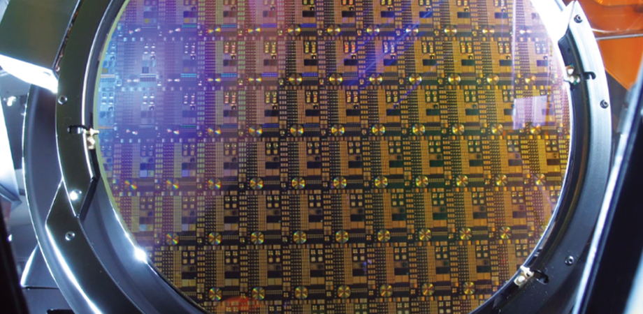
But research and development aside, metaoptics look to be on the cusp of commercialization with the first application being the hundreds-of-billions-of-dollars smart phone market. Single metaoptics lenses, fabricated on silicon wafers, have the potential to replace the several refractive lenses currently used in today’s mobile devices, eliminating the so-called smart phone camera bump.
Investment target
One company set to capture market share here is NIL Technology. In 2021, the Danish firm added €26 million to the many millions of euros it has already won in venture funds and is ready to mass produce its highly efficient, flat near infrared (NIR) metalenses, following years of development.
Depending on the application, the company’s so-called meta optical elements comprise arrays of pillars to sub-100 nm diameters with vertical sidewalls. A master metalens is manufactured via electron beam lithography and then mass-manufactured using nanoimprinting. And NIL Technology CEO and Founder, Dr. Theodor Nielsen, also highlights how his company can generate a design and make a prototype in less than two weeks.

Scanning electron microscopy image of a meta optical element from NIL Technology. Credit: NIL
“We are ready to serve the mobile phone industry and are building up capacity now,” he says. “The commercial interest is huge, and our short-term [market] is 3D sensing for mobile phones on both the front-facing and world-facing sides.”
“Metalenses reduce the number of elements in your optics system, are easier to assemble and provide more functionality,” he adds. “They give you the opportunity to rethink how you define your optical system and hold the promise of the perfect lens — perfect in the sense that they offer significantly more than the [refractive] lenses we have today.”
Nielsen’s colleague and Head of Optics at NIL Technology, Dr. Ulrich Quaade, described the technology in the "Photonic and Phononic Properties of Engineered Nanostructures XII" session at Photonics West, and looked at the company’s NIR camera module, which uses a 940 nm single metalens and NIR sensor. He also provided insight to how the metalens hits its 94% focusing efficiency — measured as the optical power transmitted to the focal spot divided by incident power on the lens element. “I’m not aware of anyone that has claimed efficiencies at this level,” says Nielsen. “So we’ve addressed the efficiency, we have a route to mass production... I believe we are successful as we have all of our design, fabrication and characterisation in-house, and I’m sure metalenses will be in smartphones in one to two years.”

Image from a near infrared imaging system using a single meta optical element surface designed for 940 nm wavelength by NIL Technology. Credit: NIL Technology
NIL Technology is not alone in its commercial aspirations. US-based fabless semiconductor business, Metalenz, the spin-out of Capasso’s Harvard group and headed up by Dr. Robert Devlin, won $10 million in funds last year from firms including Applied Ventures — the venture capital arm of Applied Materials — and Intel Capital to commercialise metaoptics technology. The company also unveiled its metaoptics-based dot projector for both structured light and time of flight 3D depth sensing in mobile phones, and signed a deal with STMicroelectronics to manufacture metaoptics technology for next-generation smart phones and other applications.
Mass production is imminent and as Devlin commented when Metalenz struck the STMicroelectronics deal: “We want to get metasurfaces out there in a very rapid way... in all of the places that you need 3D sensing.”
Unsurprisingly, Capasso is also very excited. “We have had many OEM suppliers, who are working with cell phones, talking to us at Metalenz, and [according to] our roadmap, you will see products with our actual metalenses in two to three years ,” he says.
“I believe that the smart phones of the future will become miniature spectrometers for sensing,” he adds. “We are beyond the point of no return now, and metaoptics will capture significant market share in optics primarily in consumer electronics, where you benefit from making things thinner.”
Rebecca Pool is a UK-based freelance writer. This article originally appeared in the 2022 SPIE Photonics West Show Daily.
| Enjoy this article? Get similar news in your inbox |
|


