Lithography still matters, but challenges change
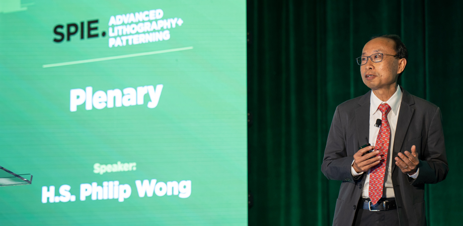
In one of two Monday morning keynotes at the SPIE Advanced Lithography and Patterning conference in San Jose, H.S. Phillip Wong, an electrical engineering professor at Stanford University and chief scientist at chip maker TSMC, posed the question: does lithography still matter? He noted that semiconductor lithography, the patterning of materials on a microscopic scale, has been a key enabler for technologies vital to the modern world.
Increasing lithographic resolution has long been a goal of equipment suppliers and chip makers because the ability to print smaller features boosts device performance while cutting cost. It’s why the industry turned to extreme ultraviolet, or EUV, lithography to produce the latest generation of chips.
But lithography is in some ways reaching the end of the road. The latest version of EUV makes it possible to pattern features only 15 atomic layers thick. So, is more lithography innovation still needed?
“The answer is yes,” Wong said near the beginning of his talk.
That innovation, though, cannot be just about resolution, he added. Throughput, the ability to handle a mix-and-match integration of different manufacturing technologies on one chip, and other factors, are growing in importance and demanding their own improvements in lithography.
For instance, there is a growing gap between how fast processing logic runs and how fast memory can supply it data. One solution is to go up, with chips composed of stacks of different subsystems atop one another.
Such an approach, though, places a premium on increasing throughput because the number of steps is greater if everything is done in one wafer fab. If manufacturing is in parallel to reduce cycle time, then the different stacks must eventually be brought together. The overlay of the various layers then becomes critical. In either case, increasing resolution will no longer be as much of an overriding goal.
The other Monday keynote also featured 3D chips and a conclusion about the need for new lithography directions. In a presentation, Luc Van den hove, president and CEO of the international research and development organization imec, spoke about the continuing prospects for Moore’s Law, and its promise of an ongoing increase in chip density.

Luc Van den hove of imec discusses the endless progression of Moore's Law. Credit: Bernd Geh
Van den hove noted that traditional scaling has been used for decades to follow Moore’s Law, and it depends on finer and finer lithographic resolution. This shrinking of dimensions, though, is running into walls. For example, there is a demand to take in more and more data and do ever more complex calculations on it. That trend cannot continue.
“If you don’t develop new technology, then the energy needed just to compute all of this data will exceed the world’s energy,” Van den hove said.
Thus, even finer lithography isn’t enough. In addition, the industry must deploy new transistor schemes, build chips in three dimensions, and switch to a more holistic approach in the design of solutions, according to Van den hove.
Each of these improvement angles brings challenges. New transistor schemes, for example, will present difficulties in learning how to manufacture devices. Building in three dimensions and with denser circuitry will make it harder to get heat out of and power into a chip. As for a more integrated approach, that requires changing how problems are solved.
“The future of scaling needs system level thinking,” said Van den hove.
The chip industry, though, has proven skilled at overcoming challenges. The number of new materials incorporated into chip manufacturing over the last 10 to 15 years is such that now the list includes most of the elements. 3D chips are already a reality in memory devices and imec, along with others, is looking at how to stack such chips atop one another.
Thus, the industry is likely to overcome these challenges, given past history and the efforts already underway. But even as lithography innovations continue and Moore’s Law marches one, don’t look for revolutionary change to happen soon, pointed out Wong.
“Technology introduction is always longer than you think,” he cautioned.
Hank Hogan is a science writer based in Reno, Nevada.
| Enjoy this article? Get similar news in your inbox |
|


