Etch: Going Up ... and Down
From talks at the Feb 2020 SPIE Advanced Lithography conference, the future of etch technology is going both up and down. So, too, is semiconductor manufacturing, with the health of the industry depending on the success of the ride.
Etch is going vertical because semiconductor devices are doing the same. Flash memory did this when it hit a wall in 2012 because it became cost prohibitive to continue shrinking the cell size in two dimensions. In response, flash memory producers transitioned to a stacked memory cell approach. Going to a 3D arrangement overcame this problem and enabled an increase in memory density, much like a change in housing increased how many people could live in a city.
"2D memory is like detached houses. 3D flash memory is like a high-rise apartment," said Mitsuhrio Omura of memory maker Kioxia in a Tuesday presentation.
There's another similarity: the aspect ratio or the height divided by the length or width of a structure. The aspect ratio of a 3D memory stack is greater than 50:1, greater than that of a skyscraper. What's more, the next generation of devices will have many more layers than today's 64 high stack of memory cells. So, the aspect ratio in 3D memory will increase.
For etch, such high aspect ratios present a challenge, one that grows along with the number of stacked layers. The etch process must tunnel down from the top of the stack to the bottom while preserving straight sides of each hole so as to minimize pinching, bowing, striations or other defects. Such defects can either cause a hole to close off or lead to one touching a neighbor. Either outcome can cause one or many memory cells to fail.
Achieving a uniform material removal rate at the top and bottom of a deep hole is difficult and the etch environment may not be uniform along the entire length. For instance, experiments by Kioxia show that during the etch process a fluorocarbon film deposits along the walls of the hole. If that film is of the right thickness, which is the case in the middle of the hole, then striations form in the film and are transferred to the walls of the hole. The resulting wall roughness is an industry concern.
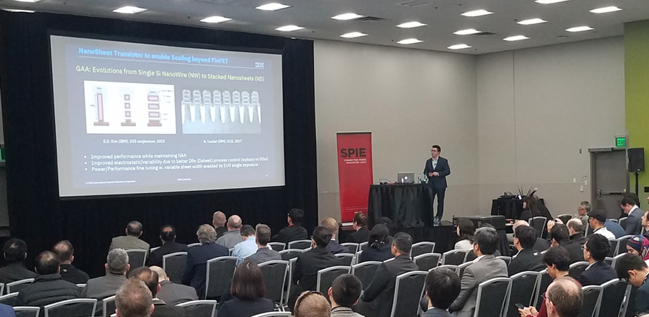
According to Omura, Kioxia is working on various solutions to the problems presented by going vertical. Whatever solution memory makers come up with may benefit logic suppliers because they too are going 3D. In a Tuesday talk, Dan Dechene, manager of DTCO and benchmarking at IBM spoke of the company's gate-all-around stacked nanosheets, a technology that IBM thinks can scale down to the 3-nm node. That is two generations beyond the 7-nm node, today's most advanced semiconductor manufacturing technology.
As is the case with stacked memory, going to 3D enables logic designs to relax some of the constraints that would otherwise be imposed by lithography. Thus, it means dimensional variability can be greater, leading to more process margin.
"In terms of having control, this is where you want to go," Dechene said.
At the same time, he added that the 3D approach does result in a high aspect ratio. It's not as large as is the case with memory. Instead of 64 layers, there are three stacks in logic, going to four in the future.
Higher aspect ratios do present challenges for etch. In overcoming those, as well as the issues associated with shrinking feature sizes in 2D situations, it will be key to look at the entire picture. Akiteru Ko, patterning etch manager at Tokyo Electron Ltd., noted that etch is done on a film that is deposited over a semiconductor chip surface. So, there are actually three sets of knobs that can be adjusted: the parameters of the etch and deposition process as well as the material characteristics of the film. Adjusting these components together can lead to better results and may be the only way to achieve the desired manufacturing outcome and chip performance.
"Continuous etch, film, and deposition holistic evaluation is required to overcome the challenges of scaling," Ko said in a Tuesday presentation.
Hank Hogan is a science writer based in Reno, Nevada.
| Enjoy this article? Get similar news in your inbox |
|


