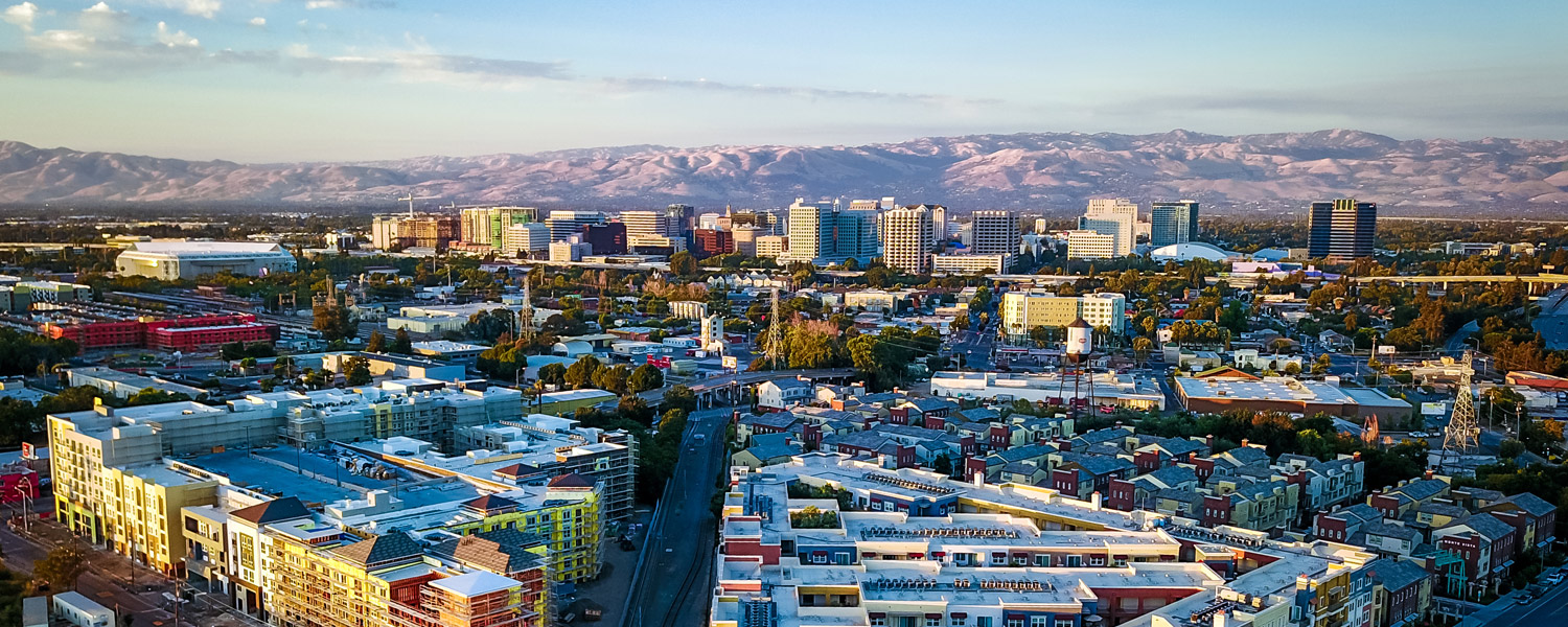
San Jose, California in the U.S. boasts the largest concentration of technology expertise in the world. San Jose also leads the nation in patent generation. The city has 25 companies with 1,000 employees or more, including the headquarters of Adobe Systems, BEA Systems, Cisco, Xilinx, Lam Research, and eBay, as well as major facilities for Flextronics, Hewlett-Packard, IBM, Hitachi, Agilent Technologies, and Lockheed Martin.
San Jose McEnery Convention Center
150 W San Carlos Street
San Jose, California 95113
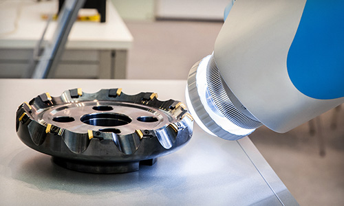
Enrich your work by attending the most important conference for optical and EUV lithography, patterning technologies, metrology, and process integration for semiconductor manufacturing and adjacent applications.
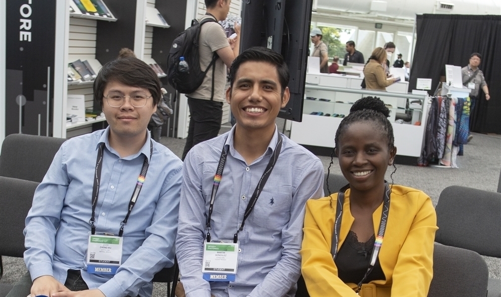
SPIE Student Members are encouraged to apply for supplemental travel grants and fee waivers to attend Advanced Lithography + Patterning. Student Members who are presenting authors will be given priority selection, but grants are open to all Student Members.