Exploring new avenues for laser micromachining
There is growing demand in several industrial sectors for instruments with a very high degree of precision, to which lasers offer the ideal solution. For a non-specialist, however, it can be difficult to identify which of the many commercially available lasers best fits their particular needs. Furthermore, the laser is generally integrated as a component in a machine that may comprise (for example) a complex optical path, galvanometric heads, and software. Laser machines are therefore expensive, and the decision to invest in one needs careful consideration.
Using lasers for manufacturing has several advantages. First, there is no contact with the material in process, and the laser system enables high accuracy, repeatability, and reproducibility. In addition, lasers offer sufficient flexibility to adapt to the parameters of the material (e.g., metal, polymer, glass, or ceramic). Continuous wave lasers are widely used for joining or direct additive laser construction (CLAD), while pulsed lasers—where thermal effects are directly linked to pulse duration—enable micromachining.1, 2 Figure 1 shows a typical laser setup for engraving.

Our collaboration of research centers and universities, known as EcoLaserFact, came together in 2012 to offer practical help to companies considering micromachining laser-based processes for their business development. The collaboration has also developed new processes for laser micro-joining, micro-fluidic devices, surface texturing, CLAD technology, and new milling systems. The group was founded by nine partners based in northwest Europe: Multitel, Sirris, and Cluster Photonics in Belgium; Karlsruhe Institute of Technology and Bayerisches Lazercentrum in Germany; the University of Birmingham and Cardiff University in the UK; and Irepa Laser and the European Photonic Industrial Consortium in France. These companies were later joined by Belgian groups Lasea and the Centre de Recherche de l'Industrie Belge de la Céramique.
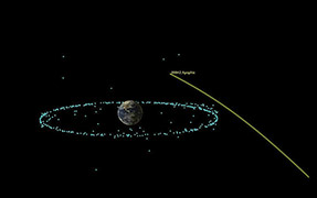
Our EcoLaserFact collaboration comprises partners involved in specific laser domains. These include subtractive manufacturing (the process of removing a material from a solid using a laser beam), additive manufacturing (layer-by-layer powder deposition and melting by lasers), material modification (local change of the intrinsic properties of the material), and joining. In fact, 61.9% of industry's demand for laser processes concerns subtractive technologies, such as marking, drilling, and engraving (see Figure 2).

Through EcoLaserFact, we train small- and medium-sized enterprises (SMEs) and universities in the basics of laser theory. We also provide an introduction to laser safety and an overview of laser processes. More than 200 people with various backgrounds have participated in our training sessions, and we have compiled (available on our website) a database containing 85 applications of microfabrication with lasers. The site also contains reports on the market and transnational collaborations between members that have led to promising new laser processes.3–6
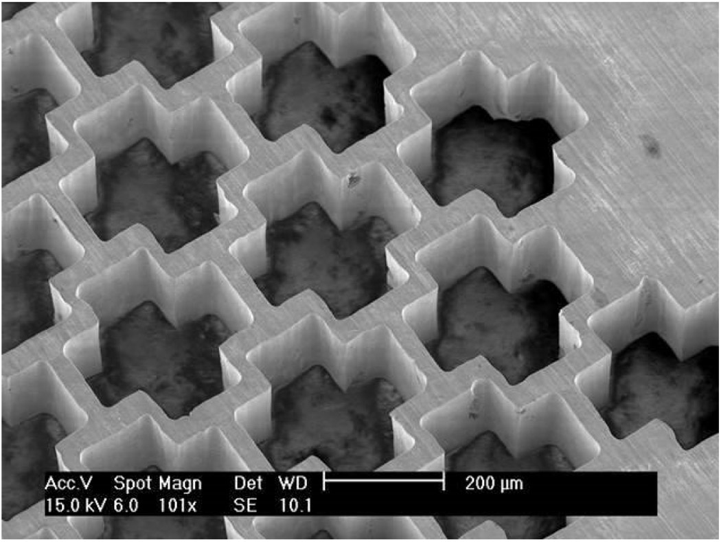
To date, we have conducted 45 feasibility studies through EcoLaserFact. These include sample demonstrations that are free of charge for SMEs in northwest Europe, which enables them to identify the most efficient technical solutions for their enterprises. Our objective is to add value through the introduction of laser technologies in production lines, leading to more customized and higher-quality products that are more environmentally friendly. For example, direct joining between metal and polymer materials is desirable to decrease the weight of workpieces and to avoid the use of chemical-containing glue. Laser surface texturing that we conducted on an aluminum sheet to obtain mechanical anchoring for thermoplastic is shown in Figure 3. Tensile tests on final, joined samples demonstrate results that are comparable with those of traditional techniques. Moreover, we can achieve complex patterning at the micrometric scale with high reproducibility (see Figure 4). We often use surface structuring to imitate nature (biomimetics). A superhydrophobic surface based on the so-called lotus effect, which has applications in the automotive and construction industries, is illustrated in Figure 5. Finally, we have also used lasers to fabricate medical components (e.g., stents and implants) and microfluidic devices (see Figure 6).


In summary, our collaboration of European research centers and universities—EcoLaserFact—was set up in 2012 to help businesses that require laser technologies. Since then, EcoLaserFact has responded to broad market interest in the use of lasers. Our next step is to offer SMEs flexible and smart laser processes. With such processes, it is possible to produce highly functional products that combine lasers and traditional technologies, such as jet printing and inline vision systems.
EcoLaserFact is supported by the European fund Interreg IV B NWE.
Anthony Bertrand joined the Applied Photonics Department in 2007. He is involved in European research and development projects, including fiber laser development and prototyping of new pulsed fiber laser sources. He is also the coordinator of the EcoLaserFact Interreg project.
Yves Hernandez leads the Applied Photonics Department. He has acted as coordinator or partner for several different European projects, and was project manager for the EcoLaserFact project.