Optipedia • SPIE Press books opened for your reference.
Line Edge Roughness
Excerpt from Field Guide to Optical Lithography
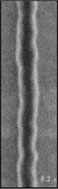 When variations in the width of a resist feature occur quickly over the length of the feature, this variation is called linewidth roughness. When examining these variations along just one edge it is called line edge roughness (LER). LER becomes important for feature sizes on the order of 100 nm or less, and can become a significant source of linewidth control problems for features below 50 nm. LER is caused by a number of statistically fluctuating effects at these small dimensions such as shot noise (photon flux variations), statistical distributions of chemical species in the resist such as photoacid generators, the random walk nature of acid diffusion during chemical amplification, and the nonzero size of resist polymers being dissolved during development. It is unclear which process or processes dominate in their contribution to LER.
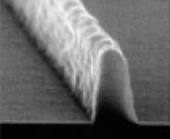 LER is usually characterized as the 3σ deviation of a line edge from a straight line, though a more complete frequency analysis of the roughness can be valuable as well. For 193-nm lithography, LER values of 4 nm and larger are common. LER is inversely proportional to the normalized image log-slope (NILS), so LER generally gets worse as an image goes out of focus and for higher resolution patterns.
The impact of LER on device performance depends on the specific device layer and specific aspects of the device technology. For lithography generations below 100 nm, typical specifications for the 3σ LER are about 5% of the nominal CD. It is possible that LER will become the main limiter of CD control below 65-nm production.
C. A. Mack, Field Guide to Optical Lithography, SPIE Press, Bellingham, WA (2006).
View SPIE terms of use.
