Optipedia • SPIE Press books opened for your reference.
Definition: Semiconductor Lithography
Excerpt from Field Guide to Optical Lithography
The fabrication of an integrated circuit (IC) requires a variety of physical and chemical processes performed on a semiconductor (e.g., silicon) substrate. In general, the various processes used to make an IC fall into three categories: film deposition, patterning, and semiconductor doping. Films of both conductors (such as polysilicon, aluminum, and more recently copper) and insulators (various forms of silicon dioxide, silicon nitride, and others) are used to connect and isolate transistors and their components. Selective doping of various regions of silicon allows the conductivity of the silicon to be changed with the application of voltage. By creating structures of these various components, millions of transistors can be built and wired together to form the complex circuitry of a modern microelectronic device. Fundamental to all of these processes is lithography, i.e., the formation of three-dimensional (3D) relief images on the substrate for subsequent transfer of the pattern to the substrate.
The word lithography comes from the Greek lithos, meaning stones, and graphia, meaning to write. It means quite literally writing on stones. In the case of semiconductor lithography, our stones are silicon wafers and our patterns are written with a light-sensitive polymer called photoresist. To build the complex structures that make up a transistor and the many wires that connect the millions of transistors of a circuit, lithography and pattern transfer steps are repeated at least 10 times, but more typically are done 20 to 30 times to make one circuit. Each pattern being printed on the wafer is aligned to the previously formed patterns and slowly the conductors, insulators, and selectively doped regions are built up to form the final device.
Overview of the Lithography Process
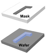
Optical lithography is a photographic process by which a light-sensitive polymer, called a photoresist, is exposed and developed to form 3D relief images on the substrate. In general, the ideal photoresist image has the exact shape of the designed or intended pattern in the plane of the substrate, with vertical walls through the thickness of the resist. Thus, the final resist pattern is binary: parts of the substrate are covered with resist while other parts are completely uncovered. This binary pattern is needed for pattern transfer since the parts of the substrate covered with resist will be protected from etching, ion implantation, or other pattern transfer mechanism.

The general sequence of steps for a typical optical lithography process is as follows: substrate preparation, photoresist spin coat, prebake, exposure, post-exposure bake, development, and postbake. A resist strip is the final operation in the lithographic process, after the resist pattern has been transferred into the underlying layer via etching or ion implantation. This sequence is generally performed on several tools linked together into a contiguous unit called a lithographic cluster.
C. A. Mack, Field Guide to Optical Lithography, SPIE Press, Bellingham, WA (2006).
View SPIE terms of use.
