What Could Kill – and Save – Moore’s Law
An as-yet-unsolved murder mystery.
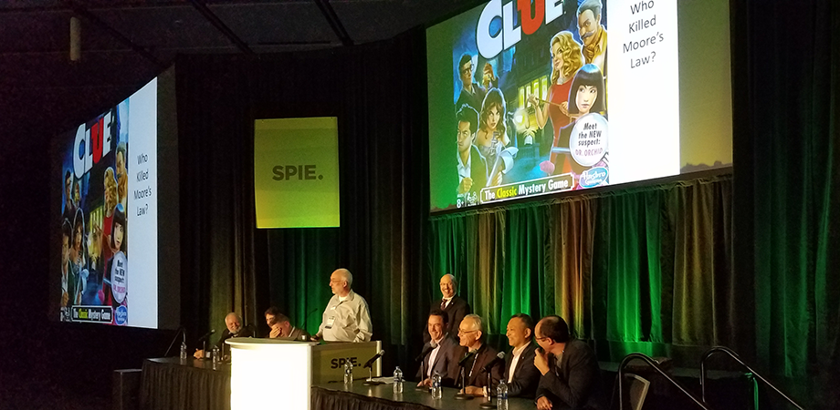
An after-hours panel discussion held at the SPIE Advanced Lithography symposium on Tuesday, 26 February sought to answer two questions: What will kill Moore's Law, and what can save it? With all seven symposium conferences represented on the panel, it seemed likely that the murder mystery would be solved. It wasn't, though, because there was no agreement about the end of Moore's Law in the first place.
The death of Moore's Law is shorthand for the end of lithographic scaling. For more than 50 years, minimum chip feature sizes have shrunk by about 12 percent a year, according to discussion moderator Chris Mack of Fractillia. That progress has slowed recently. So, is the ratcheting down of feature size over?
"It's not going to come to an end any time soon," said Tony Yen of ASML. He added that his company, which makes EUV scanners, has a 10-year roadmap of further product advances. Next up and already in development is an increase in numerical aperture from 0.33 to 0.5, which will increase resolution.
He did note that further progress will need research and development into new materials. In particular, he cited the need for new photoresists. These substances absorb incoming photons and then polymerize. This serves as a mask for etching and subsequent processing.
IMEC's John Peterson predicted that optical lithography will never hit the end of the road. Possibilities that could keep it going are machine learning and artificial intelligence, which could enhance process control and improve performance. There also could be multicolor and 3D lithography. Multicolor gives experts another knob to twist to squeeze out more performance. Going vertical changes placement constraints and is a strategy already being employed by memory chips to improve density.
His motto, Peterson said, is "optical all the way."
The question about what will save Moore's Law and lithographic scaling also brought responses that the problem would - or had - been handled.
Rob Atkin of ARM said Moore's Law had already been saved because certain scaling aspects related to processing stopped at 90 nm, or many technology nodes and more than a decade ago. However, this went unnoticed because of engineering ingenuity. "Standard cell and SRAM designers kind of hid that," he said. "It only scaled because the standard cell libraries got better."
Philip Leray of IMEC noted that if Moore's Law is slowing, there is still some significant spectrum real estate to use that could speed it back up. "There are a lot of wavelengths to be exploited and to bring value," he said.
These spectral bands could improve metrology, such as by making it easier to spot defects. A location where two metal lines almost or do touch, for instance, might be more easily found if a wafer is examined at a different wavelength or at multiple wavelengths simultaneously.
Partnerships between pairs of vendors of complementary technology could save Moore's Law, according to Rich Wise of Lam Research. The areas of beneficial back-and-forth expand with the potential solutions. An example is 3D, which presents challenges to both etch and lithography suppliers. The evolution of a combined solution was the topic of a plenary presentation by ASML and Lam Research done on Monday, 25 February.
"There are a lot of opportunities to work with your partners," Wise said.
Novel materials can help save Moore's Law, said Ryan Wilson of FUJIFILM. So, suppliers are committed to making sure the semiconductor industry has a wide range to choose from.
"We're going to keep putting forth a broad variety," Wilson said.
He also mentioned the need to better understand the stochastics, or random events, that make chemical reactions variable. That information could make it possible to tighten process specifications, thereby enabling more rigorous process control and extending scaling.
Finally, the solution to keeping Moore's Law going may entail incorporating photonics, MEMS, and other new technologies into the toolkit, said Eric Hosler of Hosler Consulting. This is because consumers don't care what the feature size is inside a chip. They only expect a certain experience with the rollout of a new technology. So long as that expectation is met, then Moore's Law, in a sense, is still alive.
But avoiding the death of Moore's Law won't be easy, according to Hosler. "It's going to involve innovation across multiple different sectors," he said.
| Panelist |
Company | Conference Represented |
| Rob Aitken | ARM | Design |
| Eric Hosler | Hosler Consulting | Novel patterning |
| Ryan Callahan | FUJIFILM | Materials |
| Rich Wise | Lam Research | Etch |
| John Petersen | IMEC | Optical lithography |
| Tony Yen | ASML | EUV |
| Philip Leray | IMEC | Metrology |
Moderators: Harry Levinson, HJL Lithography and Chris Mack, Fractillia
Hank Hogan is a science writer based in Reno, Nevada.
See more news and highlights from SPIE Advanced Lithography.
| Enjoy this article? Get similar news in your inbox |
|


