Femtoprint gets fast and furious
From precision components in breathtaking timepieces to micro-needles for vein cannulation, breakthrough laser writing from Photonics West exhibitor Femtoprint is reshaping microdevice fabrication.
Last year the Swiss watchmaker Ulysse Nardin released its extraordinary concept watch, the "InnoVision2." Replete with intricate mechanisms precisely controlling gold, silicon and sapphire parts, the timepiece stunned the world while re-plotting the future of mechanical watch making. Nestled within the watch's innovations lie two glass components; a minute hand and a balance wheel bridge. Each was fabricated by Switzerland-based laser microsystems company Femtoprint, and each follows years of painstaking research to perfect the art of rapid laser writing for watchmaking, and much more.
Femtoprint was established in 2014, following a €3.4 million, three-year European Union project, also called Femtoprint. Here, a pan-European team, including laser vendor Amplitude Systemes, microelectronics supplier Quintenz Hybridtechnik, precision mechanics devel- oper Mecartex, plus research teams at the universities of Eindhoven and Southampton, had set out to create a cost-effective tool that could convert a solid material into a microdevice without the need for a cleanroom.
As Femtoprint chief executive Nicoletta Casanova puts it: "The team wanted to create a system that would spark real innovation and rapid prototyping in univer- sities and small companies."
"Any kind of miniaturization process typically needs a cleanroom, but this is expensive, consumes large amounts of energy and many organizations just can't afford it," she says. "The idea was to develop a new tool that could convert a piece of glass into a microsystem with optical, mechanical and fluidic functionalities, without the cleanroom environment and subsequent assembly process."
At the time, many researchers had been using femtosecond lasers to micromachine 3D microstructures, writing, for example, waveguides into fused silica and borosilicate glasses. In traditional industrial laser machining, based on ablation, the smallest feature size is driven by the optical diffraction limit. But the nonlinearinteractions generated by ultrafast lasers dictate that feature sizes below the diffraction limit can be delivered.
Still, the Femtoprint researchers wanted to build on this and produce a versatile, compact machining platform that used a lower-energy femtosecond laser and was only tabletop-sized. And this is exactly what they did.
By the end of the project, the team had built a 1030 nm laser with an output below 60 mW that was smaller than a shoe box and could write microstructures within glass at sub-micron resolution and an aspect ratio better than 1:200. The laser source delivered a pulse energy of up to a microjoule, with a 600 kHz repetition rate and 300 femtosecond pulse duration. During laser exposure, that translates to instantaneous powers of a terawatt per square centimeter, but an average power of only a few hundred milliwatts: comparable to that of a bright LED.
This laser was integrated into a desktop-sized "printer", alongside piezoelectric motor-driven stages and high-accuracy beam positioning to manipulate glass sheets of different thicknesses. Software also converted 3D computer aided design files into executable machine code, ready for writing the necessary structures.
Writing with a laser
As part of the Femtoprint 3D printing process, tightly focused, low-energy femtosecond pulses below the ablation threshold are used to pattern the glass matrix. Densification within the focal point of the laser changes the properties of the glass with both the refractive index and etching rate of the material increasing.
By moving the material relative to the laser focus, microstructures are scribed into the glass and then etched with hydrofluoric acid to remove the written parts and form the 3D structure.
"We actually work with the laser inside the volume of the glass, printing what we want and then removing this drawing with a selective etching solution, which in effect sets the device free from the glass," notes Casanova.
"In this way we get the real 3D structure with, say, the necessary microfluidics and mechanics in a monolith."
Indeed, as early as 2004, members of the Femtoprint team had used femtosecond laser writing to fabricate fluidic channels and tunnels of virtually any shape within fused silica. But as the Femtoprint project progressed, increasingly novel and complex components were being rapidly prototyped. They included the first transparent actuator as well as a biochip with integrated channels and waveguides, for monitoring algae populations.
And by the end of the project, the team of researchers at the University of Southampton had showcased what was dubbed "Superman memory." The five-dimensional optical data storage format - which uses birefringence as an extra degree of freedom - comprised laser-induced nano-gratings in fused silica, and promises virtually limitless data storage.
With the compact 3D printer developed, system costs reduced, and myriad components demonstrated, the project's final objective was achieved: Femtoprint was launched as a commercial entity.
Commercial progress
With company in tow, Casanova soon realized the platform's untapped potential. "I would meet with clients and they would say, ‘I don't actually need this technology to make rapid prototypes, I need it to create devices that I just can't make with standard technologies'."
From day one, Femtoprint has been doing this and more. Recent examples include the delivery of challenging fiber alignment systems for the telecoms industry and a 3D electrode implant, while micro-tools for vein cannulation have also been developed for medical applications.
In a more unusual move, the company produced novel glass targets suspended within microfluidic chips, to investigate the effect of a swimming microbot's morphology on complex fluid flows within the chip. But in terms of sheer beauty, the best was yet to come.
Femtoprint is fabricating 3D microfluidic channel devices for microbiology research. Inset: a device for blood analysis. Photo: Femtoprint.
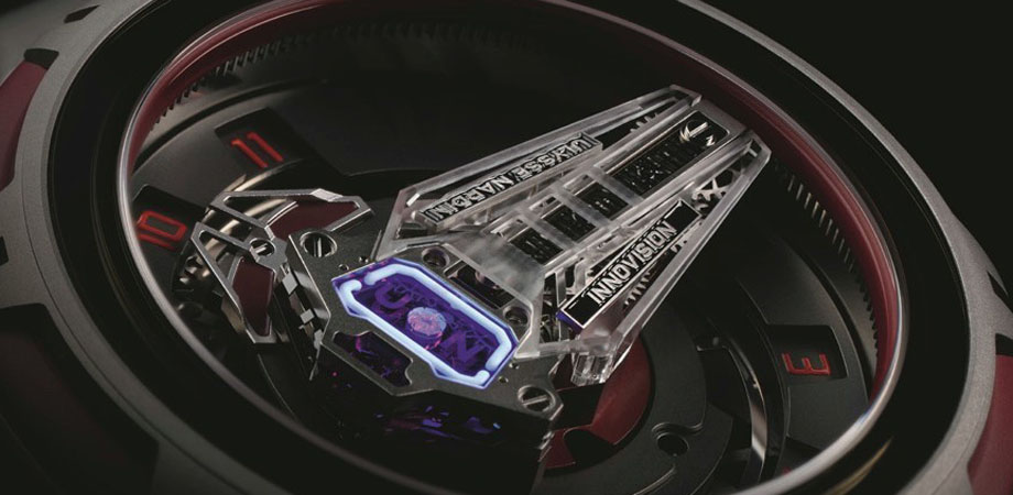
In 2017, Ulysse Nardin released the second version of what can only be described as a breathtaking concept watch, the InnoVision2. Intent on driving watch manufacturing to its limits, the Swiss firm had already become the first to use silicon in a wristwatch, and in 2007 stunned the industry with its InnoVision1. History repeated itself with last year's innovation-packed update.
Crucially for Femtoprint, the company wanted two critical 3D fused silica sculptures: a cage-shaped 3D glass minute hand, and a glass balance bridge. "[Ulysse Nardin] came to us and said, ‘we would like you to fabricate these two pieces and if you can do this all in less than a month, you have authorization to disclose them later on'," explains Casanova.
She describes the Innovision2 minute hand as "beautiful and unique", highlighting how her team laser-sculpted the delicate part and placed it on a thin metal backing to make it flexible and able to bear extreme shock. The glass balance wheel bridge, based on a monolith of fused silica, was produced in a single piece without masks, ablation, assembling, or other traditional manufacturing, and showcases exactly what the company's 3D printing process is capable of.
As part of the design, silica glass is used as the balance cock, holding and providing integrated shock protection for the balance wheel. The component contains precisely written fluidic channels, which are filled with a photoluminescent compound that exhibits a blue glow when mixed with an oxidizing agent.
The center of the bridge integrates other intricate flexures to provide additional shock resistance, while the brand letters "U" and "N" within the silica body provide a fine demonstration of 5D optical writing.
"We created the flexures to absorb shock, and removing the glass to leave these perfect flexures was a challenge," admits Casanova. "And then we altered the polarization of the material to make sure you could see the company brand.
"This project wasn't just about uploading a drawing into the system, hitting enter and getting the part," she adds. "We really had to make many iterations and push our limits, but in the end you can design any component you want inside glass, and we are now adding even more challenging components to our portfolio." 
This glass bridge of the Innovision2 watch provides integrated balance shock protection, partly thanks to laser-sculpted flexures. Photo: Ulysse Nardin.
So where next for Femtoprint? While the company continues to add to its ever-swelling collection of components and devices, it is also offering two versions of its latest 3D printer. They work with a range of transparent materials, including borosilicates and alkali-free glasses, as well as fused silica.
As Casanova points out: "Fused silica is still used in 99% of our applications, but we alter the laser power according to the type of material we are using."
The latest printers are more compact, and reach a resolution down to 0.5 microns in all three spatial directions. Thanks to ongoing software and control developments, they are ten times faster than the original project prototype and reach writing speeds of more than 140 mm/s, while still ensuring high surface quality and accuracy of the microdevices.
"Now we really are moving from rapid prototyping to serial production," Casanova says. "We have produced thousands of pieces for some of our customers.
"We have developed some key components internally, such as the stages, but we are always encouraging collaborations." she says. "We have also spent a lot of time on our software and control, but I always stress that if you can, you should work closely with experts, such as the laser manufacturers, while keeping the focus on our process; this is the path to excellence."
Rebecca Pool is a UK-based freelance writer. A version of this article appeared in the Photonics West Show Daily in January.
| Enjoy this article? Get similar news in your inbox |
|


